Advertisements
Advertisements
प्रश्न
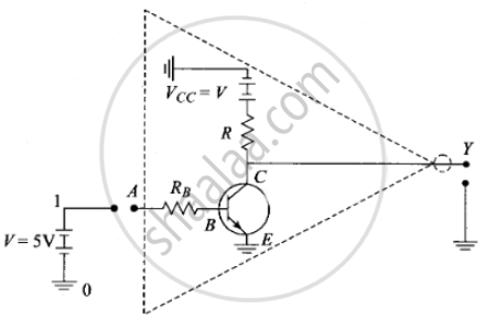
How would you set up a circuit to obtain NOT gate using a transistor?
उत्तर
(1) It has only one input and only one output.
(2) Boolean expression is Y = Ᾱ and is read as “y equals not A”.
Logical symbol of NOT gate.

(3) Realization of NOT gate: The transistor is so biased that the collector voltage VCC = V (Voltage corresponding to 1 state)
The resistors R and RB are so chosen that if the input is low, i.e. 0, the transistor is in the cut-off and hence the voltage appearing at the output will be the same as applied V = 5 V. Hence Y = V (or state I)
If the input is high, the transistor current is in saturation and the net voltage at the output Y is 0 (in state 0).

(4) Truth table for NOT gate:
| A | Y = Ā |
| 0 | 1 |
| 1 | 0 |
APPEARS IN
संबंधित प्रश्न
The output of NOR gate is high, when _______.
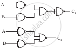
You are given two circuits as shown in following figure, which consist of NAND gates. Identify the logic operation carried out by the two circuits.
(a)

(b)

Draw the schematic symbols for AND, OR, NOT and NAND gate
What will be the values of input A and B for the Boolean expression `overline ((A +B) .(A*B)) =1?`
The outputs of two NOT gates are fed to a NOR gate. Draw the logic circuit of the combination of gates. Write its truth table. Identify the gate equivalent to this circuit.
The current obtained from a simple filterless rectifier is
Which logic gate is similar to a function of two series switches?
The truth table for the following logic circuit is:

Draw the output signals C1 and C2 in the given combination of gates (Figure).


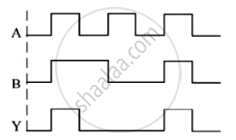
A logic gate circuit has two inputs A and B and output Y. The voltage waveforms of A, B and Y are shown below.

The logic gate circuit is ______.
