Advertisements
Advertisements
Question
How would you set up a circuit to obtain NOT gate using a transistor?
Solution
(1) It has only one input and only one output.
(2) Boolean expression is Y = Ᾱ and is read as “y equals not A”.
Logical symbol of NOT gate.

(3) Realization of NOT gate: The transistor is so biased that the collector voltage VCC = V (Voltage corresponding to 1 state)
The resistors R and RB are so chosen that if the input is low, i.e. 0, the transistor is in the cut-off and hence the voltage appearing at the output will be the same as applied V = 5 V. Hence Y = V (or state I)
If the input is high, the transistor current is in saturation and the net voltage at the output Y is 0 (in state 0).
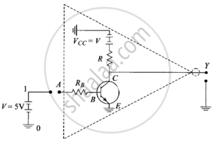
(4) Truth table for NOT gate:
| A | Y = Ā |
| 0 | 1 |
| 1 | 0 |
APPEARS IN
RELATED QUESTIONS
The output of NOR gate is high, when _______.
Let \[X = A \overline{ BC} + B\overline{ CA} + C\overline{AB } .\] Evaluate X for A = B = C = 1.
Let \[X = A \overline{ BC} + B\overline{ CA} + C\overline{AB } .\] Evaluate X for A = B = C = 0.
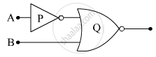
(i) Write the truth tables of the logic gates marked P and Q in the given circuit.
(ii) Write the truth table for the circuit.
With the help of a diagram, show how you can use several NAND gates to obtain an OR gate.
Useful Constants and Relations :
| 1. Speed of Light in Vacuum | (c) = 3.00 x 10⁸ m/s |
| 2. Charge of a proton | (e) = 1.60 x 10⁻¹⁹C |
| 3. Planck's Constant | (h) = 6.6 x 10⁻³⁴ Js |
| 4. Permeability of vacuum | (μ0) = 4π x 10-7 Hm-1 |
| 5. Electron Volt | (1eV ) = 1.6 x 10 |
| 6. Unified Atomic Mass Unit | (1u) = 931 MeV |
| (π) = 3.14 | |
| ( ln 2 ) = 0.693 |
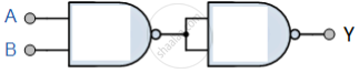
You are given circuit as shown in the figure, which consists of NAND gate. Identify the logic operation carried out by the two. Write the truth table. Identify the gates equivalent to the tow circuits.
A radar is sending out pules of 1 micro second duration at interval of 100 micro-second. The range of the radar is
Write the truth table for the circuit shown in figure. Name the gate that the circuit resembles.
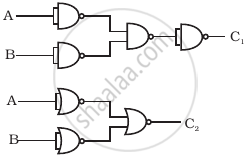
Draw the output signals C1 and C2 in the given combination of gates (Figure).

A logic gate circuit has two inputs A and B and output Y. The voltage waveforms of A, B and Y are shown below.
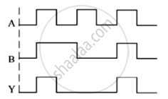
The logic gate circuit is ______.
