Advertisements
Advertisements
Question
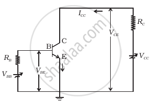
Consider the circuit arrangement shown in figure (a) for studying input and output characteristics of npn transistor in CE configuration.
 (a) |
 (b) |
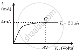
Select the values of RB and RC for a transistor whose VBE = 0.7 V, so that the transistor is operating at point Q as shown in the characteristics shown in figure (b). Given that the input impedance of the transistor is very small and VCC = VBB = 16 V, also find the voltage gain and power gain of the circuit making appropriate assumptions.
Solution
According to the problem, at point Q, from graph VBE = 0.7 V, VCC = VBB = 16 V and VCE = 8 V
IC = 4 mA = 4 × 10⁻³ A
IB = 30 μA = 30 × 10–6 A
Since, VCC = ICRC + VCE
`R_C = (V_(CC) - V_(CE))/I_C`
= `(16 - 8)/(4 xx 10^-3)`
= `(8 xx 1000)/4`
= 2 kΩ
Similarly, VBB = IBRB + VBE
`R_B = (V_(BB) - V_(BE))/I_B`
= `(16 - 0.7)/(30 xx 10^-6)`
= `510 xx 10^3` Ω
= 510 kΩ
Current gain, `β = I_C/I_B = (4 xx 10^-3)/(30 xx 10^-6)` = 133.3
Voltage gain = `β (R_C)/R_B = (133 xx 2 xx 10^3)/(510 xx 10^3)` = 0.52
Power gain = β × Voltage gain = 133 × 0.52 = 69
APPEARS IN
RELATED QUESTIONS
What are α and β parameters for a transistor? Obtain a relation between them.
Write clearly, why in the case of a transistor (i) the base is thin and lightly doped
Write clearly, why in the case of a transistor (ii) the emitter is heavily doped.
Differentiate between three segments of a transistor on the basis of their size and level of doping.
How is a transistor biased to be in active state?
When a p-n-p transistor is operated in saturation region, then its ______.
(A) base-emitter junction is forward biased and base-collector junction is reverse biased.
(B) both base-emitter and base-collector junctions are reverse biased.
(C) both base-emitter and base-collector junctions are forward biased.
(D) base-emitter junction is reverse biased and base-collector junction is forward biased
Write the functions of the three segments of a transistor.
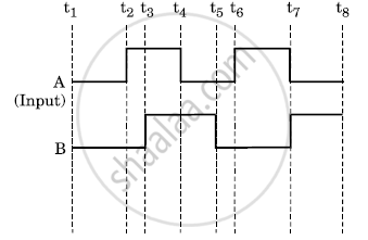
The figure shows the input waveforms A and B for ‘AND’ gate. Draw the output waveform and write the truth table for this logic gate.
Draw typical output characteristics of an n-p-n transistor in CE configuration. Show how these characteristics can be used to determine output resistance.
Sanya performed an experiment of obtaining characteristic curves of a junction diode. When she forward biased it, she found that beyond forward voltage V = Vk, the conductivity is very high. When she reverse biased the diode she found that a very small current (of about a few microamperes) flows in the diode. It remained constant even though she varied the voltage.
(i) In Figure 1 below, which one of the diodes is forward biased?
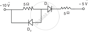
Figure 1
(ii) What is meant by a saturation current?
(iii) When applied voltage during forward bias is small, why does no current flow in the diode?
(iv) The circuit shown in Figure 2 below contains two diodes, each with a forward resistance of 50 Ω and with infinite resistance during reverse bias. If the battery voltage is 6V, then calculate the current through the 100 Ω resistance.
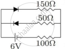
Figure 2
