Advertisements
Advertisements
Question
Distinguish between a conductor and a semi conductor on the basis of energy band diagram
Solution
Distinction between conductor and insulator:
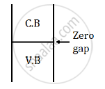
Conductor: In a conductor, the valance band is either partially filled or completely filled.
It has zero forbidden energy gap between the conduction band and the valance band.
The energy band diagram can be represented as shown below:
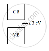
Insulator: In an insulator, the valance band is completely filled and the conduction band is empty.
The forbidden energy gap between the conduction band and the valance band is greater than or equal to 3 eV
The energy band diagram can be represented as shown below:
APPEARS IN
RELATED QUESTIONS
What is the resistance of an intrinsic semiconductor at 0 K?
In a pure semiconductor, the number of conduction election 6 × 10¹⁹ per cubic metre. How many holes are there in a sample of size 1 cm × 1 mm?
When a semiconducting material is doped with an impurity, new acceptor levels are created. In a particular thermal collision, a valence electron receives an energy equal to 2kT and just reaches one of the acceptor levels. Assuming that the energy of the electron was at the top edge of the valence band and that the temperature T is equal to 300 K, find the energy of the acceptor levels above the valence band.
Find the maximum wavelength of electromagnetic radiation which can create a hole-electron pair in germanium. The band gap in germanium is 0.65 eV.
(Use Planck constant h = 4.14 × 10⁻¹⁵ eV-s, Boltzmann constant k = 8·62 × 10-5 eV/K.)
Estimate the proportion of boron impurity which will increase the conductivity of a pure silicon sample by a factor of 100. Assume that each boron atom creates a hole and the concentration of holes in pure silicon at the same temperature is 7 × 10¹⁵ holes per cubic metre. Density of silicon 5 × 1028 atoms per cubic metre.
A semiconducting material has a band gap of 1 eV. Acceptor impurities are doped into it which create acceptor levels 1 meV above the valence band. Assume that the transition from one energy level to the other is almost forbidden if kT is less than 1/50 of the energy gap. Also if kT is more than twice the gap, the upper levels have maximum population. The temperature of the semiconductor is increased from 0 K. The concentration of the holes increases with temperature and after a certain temperature it becomes approximately constant. As the temperature is further increased, the hole concentration again starts increasing at a certain temperature. Find the order of the temperature range in which the hole concentration remains approximately constant.
(Use Planck constant h = 4.14 × 10⁻¹⁵ eV-s, Boltzmann constant k = 8·62 × 10-5 eV/K.)
If the lattice constant of this semiconductor is decreased, then which of the following is correct?
For germanium crystal, the forbidden gas energy gap
The valance of an impurity added to germanium crystal in order to convert it into p-type semiconductor is
Three photo diodes D1, D2 and D3 are made of semiconductors having band gaps of 2.5 eV, 2 eV and 3 eV, respectively. Which 0 ones will be able to detect light of wavelength 6000 Å?
