Advertisements
Advertisements
Question
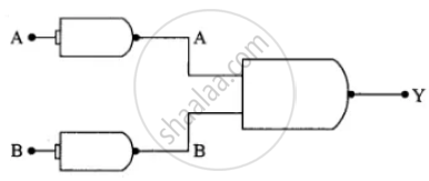
Draw a diagram to show how NAND gates can be combined to obtain an OR gate. (Truth table is not, required)
Useful Constants and Relations:
| 1. | Charge of a proton | (e) | =1.6 × 10⁻¹⁹C |
| 2. | Planck's constant | (h) | = 6·6 × 10-34 Js |
| 3. | Mass of an electron | (m) | = 9·1× 10-31 kg |
| 4. | Permittivity of vacuum | (∈0) | =8 · 85 × 10-12 Fm-1 |
| 5. | `(1/(4pi∈_0))` | =9 ×10⁹ mF-1 | |
| 6. | Permeability of vacuum | (μ0) | = 4π × 10-7 Hm-1 |
| 7. | `((mu_0)/(4pi))` | =1 × 10⁻⁷ Hm-1 | |
| 8. | Speed of light in vacuum | (c) | = 3× 10⁸ ms-1 |
| 9. | Unified atomic mass unit | (u) |
= 931 MeV |
| 10. | Electron volt | (leV) | = 1.6 × 10⁻¹⁹ J |
Solution
APPEARS IN
RELATED QUESTIONS
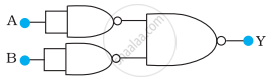
You are given two circuits as shown in following figure, which consist of NAND gates. Identify the logic operation carried out by the two circuits.
(a)
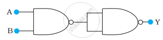
(b)
The arrangement given below represents a logic gate :
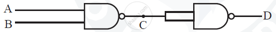
Copy the following truth table in your answer booklet and complete it showing outputs at C
and D.
| A | B | C | D |
| 0 | 0 | ||
| 1 | 0 | ||
| 0 | 1 | ||
| 1 | 0 |
The output of an OR gate is connected to both the inputs of a NAND gate Draw the logic circuit of this combinaion of getes and write its truth table.
An AND gate can be prepared by repetitive use of
(a) NOT gate
(b) OR gate
(c) NAND gate
(d) NOR gate.
Let \[X = A \overline{ BC} + B\overline{ CA} + C\overline{AB } .\] Evaluate X for A = 1, B = 0, C = 1.
Let \[X = A \overline{ BC} + B\overline{ CA} + C\overline{AB } .\] Evaluate X for A = B = C = 0.
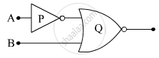
(i) Write the truth tables of the logic gates marked P and Q in the given circuit.
(ii) Write the truth table for the circuit.
With the help of a diagram, show how you can use several NAND gates to obtain an OR gate.
Useful Constants and Relations :
| 1. Speed of Light in Vacuum | (c) = 3.00 x 10⁸ m/s |
| 2. Charge of a proton | (e) = 1.60 x 10⁻¹⁹C |
| 3. Planck's Constant | (h) = 6.6 x 10⁻³⁴ Js |
| 4. Permeability of vacuum | (μ0) = 4π x 10-7 Hm-1 |
| 5. Electron Volt | (1eV ) = 1.6 x 10 |
| 6. Unified Atomic Mass Unit | (1u) = 931 MeV |
| (π) = 3.14 | |
| ( ln 2 ) = 0.693 |
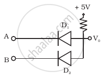
Write the truth table for the circuit shown in figure. Name the gate that the circuit resembles.
A logic gate circuit has two inputs A and B and output Y. The voltage waveforms of A, B and Y are shown below.
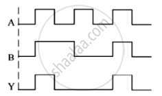
The logic gate circuit is ______.
