Advertisements
Advertisements
Question
Draw a circuit diagram of an n-p-n transistor with its emitter-base junction forward biased and basecollector junction reverse biased. Briefly describe its working.
Explain how a transistor in its active state exhibits a low resistance at its emitter-base junction and high resistance at its base-collector junction.
Solution
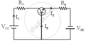
Working: The heavily doped emitter has a high concentration of majority carriers, which is electrons in
an n-p-n transistor. These majority carriers enter the base region in large numbers. The base is thin and lightly doped. So the majority carriers there would be few. The large number of electrons entering the base from the emitter swamps the small number of holes there. As the base collector junction is reverse biased, these electrons which appear as minority carriers at the junction, can easily cross the junction and enter into the collector and reach the collector terminal. The base is made thin so that most of the electrons find themselves near the reverse biased base collector junction and so cross the junction instead of moving to the base terminal. The direction of currents will be opposite to the direction of flow of electrons, which is shown in the figure. Thus, emitter current is the sum of collector current and base current. While using a transistor, the emitter base junction is always forward biased and collector base junction is always reverse biased. Due to this, a small change in emitter voltage produces a large change in emitter current in active state. This means that a small signal voltage variation at the input of the transistor produces a large emitter current variation. This shows that the input resistance of the transistor is low. Since collector base junction is reverse biased, it collects all the charge carriers which diffuse into if, through base. Due to this, a very large change in collector voltage shows only a small change in the collector current. This shows that the output resistance of the transistor is high.
APPEARS IN
RELATED QUESTIONS
Draw a simple circuit of a CE transistor amplifier. Explain its working ?
Show that the voltage gain, AV, of the amplifier is given by `A_v = (beta_(ac) R_1)/r_i`where βac is the current gain, RL is the load resistance and ri is the input resistance of the transistor. What is the significance of the negative sign in the expression for the voltage gain?
Let iE, iC and iB represent the emitter current, the collector current and the base current respectively in a transistor. Then
(a) iC is slightly smaller than iE
(b) iC is slightly greater than iE
(c) iB is much smaller than iE
(d) iB is much greater than iE.
In a normal operation of a transistor,
(a) the base−emitter junction is forward-baised
(b) the base−collector junction is forward-baised
(c) the base−emitter junction is reverse-baised
(d) the base−collector junction is reverse-baised.
Derive the expression for the voltage gain of a transistor amplifier in CE configuration in terms of the load resistance RL, current gain a βa and input resistance.
Explain why input and output voltages are in opposite phase.
Draw a circuit diagram of an n-p-n transistor with its emitter-base junction forward biased and base-collector junction reverse biased. Briefly describe its working.
Explain how a transistor in its active state exhibits a low resistance at its emitter-base junction and high resistance at its base-collector junction.
Derive the expression for the voltage gain of a transistor amplifier in CE configuration in terms of the load resistance RL, current gain βa and input resistance.
Explain why input and output voltages are in the opposite phase.
Answer the following question.
Draw the circuit arrangement for studying the output characteristics of an n-p-n transistor in CE configuration. Explain how the output characteristics is obtained.
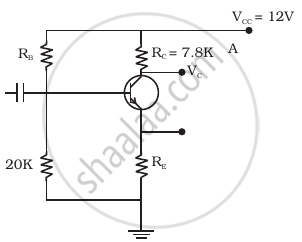
For the transistor circuit shown in figure, evaluate VE, RB, RE given IC = 1 mA, VCE = 3 V, VBE = 0.5 V and VCC = 12 V, β = 100.