Advertisements
Advertisements
Questions
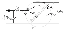
Draw a circuit diagram of a transistor amplifier in CE configuration.
Draw a circuit diagram of n-p-n transistor amplifier in CE configuration
Solution
The circuit diagram of an NPN transistor amplifier in CE configuration is given below:
APPEARS IN
RELATED QUESTIONS
Draw a circuit diagram of a p-n-p transistor and explain how it works as a transistor amplifier
Under what condition does the transistor act as an amplifier?
Draw a circuit diagram for studying the input and output characteristics of a n-p-n transistor in common emitter configuration. Using the circuit, explain how input, output characteristics are obtained
Draw a labelled diagram of a common emitter amplifier, showing waveforms of the signal voltage and output voltage.
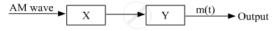
Figure shows a block diagram of a detector for amplitude modulated signal. Identify the boxes ‘X’ and ‘Y’ and write their functions.
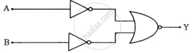
Write the truth table of the following circuit. Name the gate represented by this circuit.
In a common base amplifier, the phase difference between the input signal voltage and output voltage is ______.
In common emitter amplifier, the current gain is 62. The collector resistance and input resistance are 5 kΩ and 500 Ω respectively. If the input voltage is 0.01 V, the output voltage is:
A pnp transistor is used in common-emitter mode in an amplifier circuit. A change of 40 µA in the base current brings a change of 2 mA in collector current and 0.04 V in base emitter voltage. Which of the following is the correct value of the input resistor Rin?
When a junction transistor is used as an amplifier in CE-mode,
