Advertisements
Advertisements
Question
Explain the principle of operation of a photodiode.
Solution 1
Construction: A photodiode consists of an n-type silicon substrate with a metal electrode back contact. A thin p-type layer is grown over the n-type substrate by diffusing a suitable acceptor dopant.
The area of the player defines the photodiode active area. An ohmic contact pad is deposited on the active area. The rest of the active area is left open with a protective anti-reflective coating of silicon nitride to minimize the loss of photons. The nonactive area is covered with an insulating opaque SiO2 coating.

(a) Planar photodiode (b) Circuit symbol
Depending on the required spectral sensitivity, i.e., the operating wavelength range, typical photodiode materials are silicon, germanium, indium gallium arsenide phosphide (InGaAsP), and indium gallium arsenide (InGaAs), of which silicon is the cheapest while the last two are expensive.
Working: The band gap energy of silicon is EG = 1.12 eV at room temperature. Thus, photons or particles with energies greater than or equal to 1.12 eV, which corresponds to λ ≤ 10 nm, can transfer electrons from the valence band into the conduction band.
A photodiode is operated in the reverse bias mode which results in a wider depletion region. When operated in the dark (zero illumination), there is a reverse saturation current due solely to the thermally generated minority charge carriers. This is called the dark current. Depending on the minority carrier concentrations, the dark current in an Si photodiode may range from 5 pA to 10 nA.
When exposed to radiation of energy hv ≥ EG (in the range near-UV to near-IR), electron-hole pairs are created in the depletion region. The electric field in the depletion layer accelerates these photogenerated electrons and holes towards the n side and p side, respectively, constituting a photocurrent I in the external circuit from the p side to the n side. Due to the photogeneration, more charge carriers are available for conduction and the reverse current is increased. The photocurrent is directly proportional to the intensity of the incident light. It is independent of the reverse bias voltage.
- silicon (Si): low dark current, high speed, good sensitivity between ∼ 400 nm and 1000 nm (best around 800 nm-900 nm)
- germanium (Ge): high dark current, slow speed, good sensitivity between ∼ 900 nm and 1600 nm (best around 1400 nm-1500 nm)
- indium gallium arsenide phosphide (InGaAsP): expensive, low dark current, high speed, good sensitivity between ∼1000 nm and 1350 nm (best around 1100 run-1300 nm)
- indium gallium arsenide (InGaAs): expensive, low dark current, high speed, good sensitivity between ∼900 nm and 1700 nm (best around 1300 nm-1600 nm].
Solution 2
Working principle of photodiode:
- When a p-n junction diode is reverse biased, a reverse saturation current flows through the junction.
- The magnitude of this current is constant for a certain range of reverse bias voltages. This current is due to the minority carriers on either side of the junction. The figure shows a schematic representation of the working of a photodiode.

Working on a photodiode - The reverse current depends only on the concentration of the minority carriers and not on the applied voltage. This reverse current is called dark current because it flows even when the photodiode is not illuminated.
- When the p-n junction is illuminated with photons of energy greater than the bandgap energy of semiconductor electron-hole pairs is generated in the depletion region.
- The electrons and the holes are separated due to the intrinsic electric field present in the depletion region. The electrons are attracted towards the anode and the holes are attracted towards the cathode. More carriers are available for conduction and the reverse current is increased.
- The reverse current of a photodiode depends on the intensity of the incident light. Thus, the reverse current can be controlled by controlling the concentration of the minority carriers in the junction.
APPEARS IN
RELATED QUESTIONS
Choose the correct option:
A Series resistance is connected in the Zener diode circuit to ______.
An LED emits visible light when it's ______.
Answer in brief.
On which factors does the wavelength of light emitted by a LED depend?
State the principle of solar cells.
Explain how a Zener diode maintains a constant voltage across a load.
Explain the forward and the reverse characteristic of a Zener diode.
Explain the working of a LED.
State any two special-purpose diodes.
State any two advantages and disadvantages of a photodiode.
Define the dark current of the photodiode. What are the advantages and disadvantages of a photodiode?
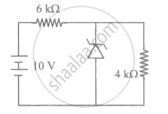
What will be the current flowing through the 6 kΩ resistor in the circuit shown, where the breakdown voltage of the Zener is 6V?
With forward biased mode, the p-n junction diode ______.
With a neat labelled diagram, explain the working of a photodiode. Calculate the wavelength in angstrom at which the emissive power is maximum for a blackbody heated to 3727 °C.
State the factors which control the wavelength of light emitte d by an LED.
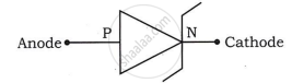
Give the name of the following symbol.
Draw a neat labelled schematic diagram of LED.
Distinguish between light-emitting diode and photo-diode.
What is Avalanche breakdown?
What is a Light Emitting Diode?
Draw Light Emitting Diode circuit symbol.
