Advertisements
Advertisements
Question
The outputs of two NOT gates are fed to a NOR gate. Draw the logic circuit of the combination of gates. Write its truth table. Identify the gate equivalent to this circuit.
Solution
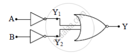
`"Y"_1 = bar"A"`
`"Y"_2 = bar"B"`
`"Y" = overline("Y"_1+"Y"_2) = overline(bar"A"+bar"B") = underset(A)(=) underset(B)(=) = "A.B"`
he equivalent gate is AND gate
Truth table
| A | B | Y1 | Y2 | Y |
| 0 | 0 | 1 | 1 | 0 |
| 0 | 1 | 1 | 0 | 0 |
| 1 | 0 | 0 | 1 | 0 |
| 1 | 1 | 0 | 0 | 1 |
APPEARS IN
RELATED QUESTIONS
Write the truth table for circuit given in figure below consisting of NOR gates and identify the logic operation (OR, AND, NOT) which this circuit is performing.
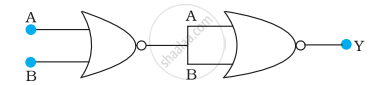
(Hint: A = 0, B = 1 then A and B inputs of second NOR gate will be 0 and hence Y=1. Similarly work out the values of Y for other combinations of A and B. Compare with the truth table of OR, AND, NOT gates and find the correct one.)
The arrangement given below represents a logic gate :
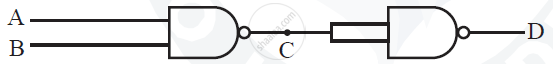
Copy the following truth table in your answer booklet and complete it showing outputs at C
and D.
| A | B | C | D |
| 0 | 0 | ||
| 1 | 0 | ||
| 0 | 1 | ||
| 1 | 0 |
Draw logic symbol of an OR gate and write its truth table.
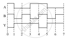
The following figure shows the input waveforms (A, B) and the output waveform (Y) of a gate. Identify the gate, write its truth table and draw its logic symbol.
Show the variation of voltage with time, for a digital signal.
NAND and NOR gates are called universal gates primarily because they ______.
The current obtained from a simple filterless rectifier is
In potential barrier development in a junction diode opposes
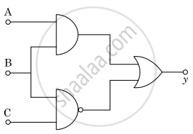
For the given circuit, the input digital signals are applied at terminals A, B, and C. What would be the output at terminal y?
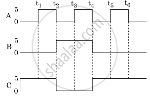
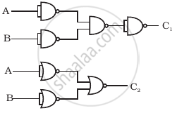
Draw the output signals C1 and C2 in the given combination of gates (Figure).