Advertisements
Advertisements
प्रश्न
Describe briefly the following term:
minority carrier injection in forward biasing.
उत्तर
Due to the applied voltage, electrons from the n-side cross the depletion region and reach the p-side (where they are minority carriers). Similarly, holes from the p-side cross this junction and reach the n-side (where they are minority carriers). This process under forward bias is known as minority carrier injection.
APPEARS IN
संबंधित प्रश्न
(i) Explain with the help of a diagram the formation of depletion region and barrier potential in a pn junction.
Plot a graph showing variation of current versus voltage for the material GaAs ?
A triode value operates at Vp = 225 V and Vg = −0.5 V.
The plate current remains unchanged if the plate voltage is increased to 250 V and the grid voltage is decreased to −2.5 V. Calculate the amplification factor.
On increasing the reverse biases voltage to a large value in a P – N junction diode-current
In a semiconductor diode, the barrier potential offers opposition to only
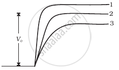
In Figure, Vo is the potential barrier across a p-n junction, when no battery is connected across the junction ______.

When an electric field is applied across a semiconductor ______.
- electrons move from lower energy level to higher energy level in the conduction band.
- electrons move from higher energy level to lower energy level in the conduction band.
- holes in the valence band move from higher energy level to lower energy level.
- holes in the valence band move from lower energy level to higher energy level.
Figure shows the transfer characteristics of a base biased CE transistor. Which of the following statements are true?

At Vi = 0.4 V, transistor is in active state.
At Vi = 1 V, it can be used as an amplifier.
At Vi = 0.5 V, it can be used as a switch turned off.
At Vi = 2.5 V, it can be used as a switch turned on.
A semiconductor device is connected in series with a battery, an ammeter and a resistor. A current flows in the circuit. If. the polarity of the battery is reversed, the current in the circuit almost becomes zero. The device is a/an ______.
Draw a labelled characteristic curve (l-V graph) for a semiconductor diode during forward bias.
