Advertisements
Advertisements
प्रश्न
Explain briefly with the help of necessary diagrams, the reverse biasing of a p-n junction diode. Also draw characteristic curves.
उत्तर
p-n junction diode under reverse bias
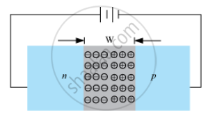
Positive terminal of battery is connected to n-side and negative terminal to p-side.
Reverse bias supports the potential barrier. Therefore, the barrier height increases and the width of depletion region also increases.
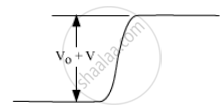
Effective barrier height under reverse bias is (V0 + V).
No conduction across the junction due to majority carriers; few minority carriers cross the junction after being accelerated by high reverse bias voltage
This constitutes a current that flows in opposite direction − celled reverse current.

APPEARS IN
संबंधित प्रश्न
Explain briefly with the help of necessary diagrams, the forward biasing of a p-n junction diode. Also draw characteristic curves.
Draw a circuit diagram to study the input and output characteristics of an n-p-n transistor in its common emitter configuration. Draw the typical input and output characteristics.
The drift current in a p-n junction is
In a p.n junction, the depletion region is 400 nm wide and an electric field of 5 × 10⁵ V m−1 exists in it. (a) Find the height of the potential barrier. (b) What should be the minimum kinetic energy of a conduction electron which can diffuse from the n-side to the p-side?
The current−voltage characteristic of an ideal p-n junction diode is given by \[i = i_0 ( e^{eV/KT} - 1)\] where, the drift current i0 equals 10 µA. Take the temperature T to be 300 K. (a) Find the voltage V0 for which \[e^{eV/kT} = 100 .\]One can neglect the term 1 for voltages greater than this value. (b) Find an expression for the dynamic resistance of the diode as a function of V for V > V0. (c) Find the voltage for which the dynamic resistance is 0.2 Ω.
(Use Planck constant h = 4.14 × 10⁻¹⁵ eV-s, Boltzmann constant k = 8·62 × 10-5 eV/K.)
When the base current in a transistor is changed from 30µA to 80µA, the collector current is changed from 1.0 mA to 3.5 mA. Find the current gain β.
A load resistor of 2kΩ is connected in the collector branch of an amplifier circuit using a transistor in common-emitter mode. The current gain β = 50. The input resistance of the transistor is 0.50 kΩ. If the input current is changed by 50µA. (a) by what amount does the output voltage change, (b) by what amount does the input voltage change and (c) what is the power gain?
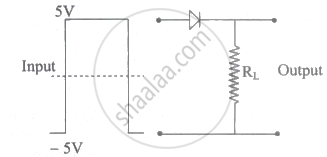
If in a p-n junction diode, a square input signal of 10 V is applied as shown Then the output signal across RL will be ______
The depletion layer in the p-n junction diode is caused by ______.
The formation of the depletion region in a p-n junction diode is due to ______.
