Advertisements
Advertisements
प्रश्न
Explain, with the help of a circuit diagram, the working of n-p-n transistor as a common emitter amplifier.
APPEARS IN
संबंधित प्रश्न
In an unbiased p-n junction, holes diffuse from the p-region to n-region because ______.
Explain briefly with the help of necessary diagrams, the reverse biasing of a p-n junction diode. Also draw characteristic curves.
A student wants to use two p-n junction diodes to convert alternating current into direct current. Draw the labelled circuit diagram she would use and explain how it works.
Mention the important considerations required while fabricating a p-n junction diode to be used as a Light Emitting Diode (LED). What should be the order of band gap of an LED if it is required to emit light in the visible range?
The diffusion current in a p-n junction is
In a p.n junction, the depletion region is 400 nm wide and an electric field of 5 × 10⁵ V m−1 exists in it. (a) Find the height of the potential barrier. (b) What should be the minimum kinetic energy of a conduction electron which can diffuse from the n-side to the p-side?
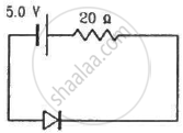
Calculate the current through the circuit and the potential difference across the diode shown in figure. The drift current for the diode is 20 µA.

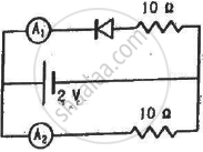
What are the readings of the ammeters A1 and A2 shown in figure. Neglect the resistance of the meters.

(Assume that the resistance of each diode is zero in forward bias and is infinity in reverse bias.)
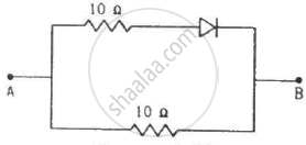
Find the equivalent resistance of the network shown in figure between the points A and B.

(Assume that the resistance of each diode is zero in forward bias and is infinity in reverse bias.)
The formation of the depletion region in a p-n junction diode is due to ______.
