Advertisements
Advertisements
प्रश्न
Explain, with the help of a circuit diagram, the working of n-p-n transistor as a common emitter amplifier.
APPEARS IN
संबंधित प्रश्न
A zener diode is fabricated by heavily doping both p- and n- sides of the junction. Explain, why?
Explain, with the help of a circuit diagram, the working of a photo-diode. Write briefly how it is used to detect the optical signals.
How is a zener diode fabricated so as to make it a special purpose diode? Draw I-V characteristics of zener diode and explain the significance of breakdown voltage.
Explain briefly, with the help of a circuit diagram, how a p-n junction diode works as a half wave rectifier.
When a p-type impurity is doped in a semiconductor, a large number of holes are created, This does not make the semiconductor charged. But when holes diffuse from the p-side to the n-side in a p-n junction, the n-side gets positively charged. Explain.
A hole diffuses from the p-side to the n-side in a p-n junction. This means that
In a p-n junction,
(a) new holes and conduction electrons are produced continuously throughout the material
(b) new holes and conduction electrons are produced continuously throughout the material except in the depletion region
(c) holes and conduction electrons recombine continuously throughout the material
(d) holes and conduction electrons recombine continuously throughout the material except in the depletion region.
A semiconducting device is connected in a series circuit with a battery and a resistance. A current is found to pass through the circuit. If the polarity of the battery is reversed, the current drops to almost zero. the device may be
(a) an intrinsic semiconductor
(b) a p-type semiconductor
(c) an n-type semiconductor
(d) a p-n junction
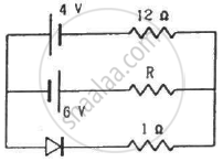
Find the current through the resistance R in figure if (a) R = 12Ω (b) R = 48Ω.

(Assume that the resistance of each diode is zero in forward bias and is infinity in reverse bias.)
p-n junction diode is formed
During the formation of a p-n junction ______.
