Advertisements
Advertisements
प्रश्न
A hole diffuses from the p-side to the n-side in a p-n junction. This means that
विकल्प
a bond is broken on the n-side and the electron freed from the bond jumps to the conduction band
a conduction electron on the p-side jumps to a broken bond to complete it
a bond is broken on the n-side and the electron freed from the bond jumps to a broken bond on the p-side to complete it
a bond is broken on the p-side and the electron freed from the bond jumps to a broken bond on the n-side to complete it.
उत्तर
a bond is broken on the n-side and the electron freed from the bond jumps to a broken bond on the p-side to complete it
A hole diffuses from the p side to the n side in a p−n junction; that is, an electron moves from the n side to the p side. This implies that a bond is broken on the n side. As the electron travels towards the p side, which is rich in holes, it combines with a hole. A hole is created because of the deficiency of one electron. So, when an electron combines with a hole, it completes that bond.
APPEARS IN
संबंधित प्रश्न
Draw a circuit diagram to study the input and output characteristics of an n-p-n transistor in its common emitter configuration. Draw the typical input and output characteristics.
The drift current in a reverse-biased p-n junction is increased in magnitude if the temperature of the junction is increased. Explain this on the basis of creation of hole-electron pairs.
If the two ends of a p-n junction are joined by a wire,
Diffusion current in a p-n junction is greater than the drift current in magnitude
In a p-n junction with open ends,
(a) there is no systematic motion of charge carries
(b) holes and conduction electrons systematically go from the p-side to n-side and from the n-side to p-side respectively
(c) there is no net charge transfer between the two sides
(d) there is a constant electric field near the junction.
In a p-n junction,
(a) new holes and conduction electrons are produced continuously throughout the material
(b) new holes and conduction electrons are produced continuously throughout the material except in the depletion region
(c) holes and conduction electrons recombine continuously throughout the material
(d) holes and conduction electrons recombine continuously throughout the material except in the depletion region.
The drift current in a p-n junction is 20.0 µA. Estimate the number of electrons crossing a cross section per second in the depletion region.
Consider a p-n junction diode having the characteristic \[i - i_0 ( e^{eV/kT} - 1) \text{ where } i_0 = 20\mu A\] . The diode is operated at T = 300 K . (a) Find the current through the diode when a voltage of 300 mV is applied across it in forward bias. (b) At what voltage does the current double?
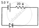
Calculate the current through the circuit and the potential difference across the diode shown in figure. The drift current for the diode is 20 µA.
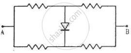
Each of the resistance shown in figure has a value of 20 Ω. Find the equivalent resistance between A and B. Does it depend on whether the point A or B is at higher potential?
What are the readings of the ammeters A1 and A2 shown in figure. Neglect the resistance of the meters.
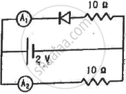
(Assume that the resistance of each diode is zero in forward bias and is infinity in reverse bias.)
Find the current through the resistance R in figure if (a) R = 12Ω (b) R = 48Ω.
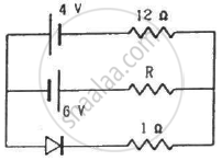
(Assume that the resistance of each diode is zero in forward bias and is infinity in reverse bias.)
Draw the current-voltage characteristics for the device show in figure between the terminals A and B.

(Assume that the resistance of each diode is zero in forward bias and is infinity in reverse bias.)
Find the equivalent resistance of the network shown in figure between the points A and B.
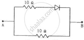
(Assume that the resistance of each diode is zero in forward bias and is infinity in reverse bias.)
A load resistor of 2kΩ is connected in the collector branch of an amplifier circuit using a transistor in common-emitter mode. The current gain β = 50. The input resistance of the transistor is 0.50 kΩ. If the input current is changed by 50µA. (a) by what amount does the output voltage change, (b) by what amount does the input voltage change and (c) what is the power gain?
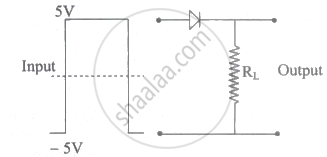
If in a p-n junction diode, a square input signal of 10 V is applied as shown Then the output signal across RL will be ______
In a semiconductor diode, the barrier potential offers opposition to only ______.
Zener breakdown occurs in a p-n junction having p and n both:
During the formation of a p-n junction ______.
