Advertisements
Advertisements
प्रश्न
In a p-n junction with open ends,
(a) there is no systematic motion of charge carries
(b) holes and conduction electrons systematically go from the p-side to n-side and from the n-side to p-side respectively
(c) there is no net charge transfer between the two sides
(d) there is a constant electric field near the junction.
उत्तर
(b) holes and conduction electrons systematically go from the p-side to n-side and from the n-side to p-side, respectively
(c) there is no net charge transfer between the two sides
(d) there is a constant electric field near the junction
Because of the difference in the concentration of charge carriers in the p−n junction, holes from the p side move to the n side and electrons from the n side move to the pside. This motion of charge carriers gives rise to diffusion current.
Because of this, a negative space charge region is formed in the p region and a positive space region is formed in the n region. This sets up an electric field across the junction. Thus, there is a constant electric field near the junction.
This electric field further opposes the diffusion of majority charge carriers across the junction. As a result, an electron from the p region starts moving to the n region and a hole from the n region starts moving to the p region. This sets up drift current. Thus, there is a systematic flow of charge carriers across the junction. Also, there is no net charge transfer between the two sides.
APPEARS IN
संबंधित प्रश्न
A zener diode is fabricated by heavily doping both p- and n- sides of the junction. Explain, why?
Explain, with the help of a circuit diagram, the working of a photo-diode. Write briefly how it is used to detect the optical signals.
The drift current in a reverse-biased p-n junction is increased in magnitude if the temperature of the junction is increased. Explain this on the basis of creation of hole-electron pairs.
Diffusion current in a p-n junction is greater than the drift current in magnitude
Two identical p-n junction may be connected in series with a battery in three ways. The potential difference across the two p-n junctions are equal in

In a p-n junction,
(a) new holes and conduction electrons are produced continuously throughout the material
(b) new holes and conduction electrons are produced continuously throughout the material except in the depletion region
(c) holes and conduction electrons recombine continuously throughout the material
(d) holes and conduction electrons recombine continuously throughout the material except in the depletion region.
In a p-n junction, a potential barrier of 250 meV exists across the junction. A hole with a kinetic energy of 300 meV approaches the junction. Find the kinetic energy of the hole when it crosses the junction if the hole approached the junction (a) from the p-side and (b) from the n-side.
The drift current in a p-n junction is 20.0 µA. Estimate the number of electrons crossing a cross section per second in the depletion region.
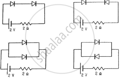
Find the currents through the resistance in the circuits shown in figure.

(Assume that the resistance of each diode is zero in forward bias and is infinity in reverse bias.)
When the base current in a transistor is changed from 30µA to 80µA, the collector current is changed from 1.0 mA to 3.5 mA. Find the current gain β.
An AC source is connected to a diode and a resistor in series. Is the current thorough the resistor AC or DC?
A diode, a resistor and a 50 Hz AC source are connected in series. The number of current pulses per second through the resistor is __________ .
Answer in detail.
Discuss the effect of external voltage on the width of depletion region of a p-n junction.
In a semiconductor diode, the barrier potential offers opposition to only ______.
p-n junction diode is formed
The formation of the depletion region in a p-n junction diode is due to ______.
During the formation of a p-n junction ______.
