Advertisements
Advertisements
प्रश्न
In a p-n junction with open ends,
(a) there is no systematic motion of charge carries
(b) holes and conduction electrons systematically go from the p-side to n-side and from the n-side to p-side respectively
(c) there is no net charge transfer between the two sides
(d) there is a constant electric field near the junction.
उत्तर
(b) holes and conduction electrons systematically go from the p-side to n-side and from the n-side to p-side, respectively
(c) there is no net charge transfer between the two sides
(d) there is a constant electric field near the junction
Because of the difference in the concentration of charge carriers in the p−n junction, holes from the p side move to the n side and electrons from the n side move to the pside. This motion of charge carriers gives rise to diffusion current.
Because of this, a negative space charge region is formed in the p region and a positive space region is formed in the n region. This sets up an electric field across the junction. Thus, there is a constant electric field near the junction.
This electric field further opposes the diffusion of majority charge carriers across the junction. As a result, an electron from the p region starts moving to the n region and a hole from the n region starts moving to the p region. This sets up drift current. Thus, there is a systematic flow of charge carriers across the junction. Also, there is no net charge transfer between the two sides.
APPEARS IN
संबंधित प्रश्न
In a p-n junction diode, the current I can be expressed as
I = `"I"_0 exp ("eV"/(2"k"_"BT") - 1)`
where I0 is called the reverse saturation current, V is the voltage across the diode and is positive for forward bias and negative for reverse bias, and I is the current through the diode, kBis the Boltzmann constant (8.6×10⁻⁵ eV/K) and T is the absolute temperature. If for a given diode I0 = 5 × 10⁻¹² A and T = 300 K, then
(a) What will be the forward current at a forward voltage of 0.6 V?
(b) What will be the increase in the current if the voltage across the diode is increased to 0.7 V?
(c) What is the dynamic resistance?
(d) What will be the current if reverse bias voltage changes from 1 V to 2 V?
Explain briefly with the help of necessary diagrams, the reverse biasing of a p-n junction diode. Also draw characteristic curves.
Draw a circuit diagram to study the input and output characteristics of an n-p-n transistor in its common emitter configuration. Draw the typical input and output characteristics.
Explain, with the help of a circuit diagram, the working of n-p-n transistor as a common emitter amplifier.
When a p-type impurity is doped in a semiconductor, a large number of holes are created, This does not make the semiconductor charged. But when holes diffuse from the p-side to the n-side in a p-n junction, the n-side gets positively charged. Explain.
The drift current in a reverse-biased p-n junction is increased in magnitude if the temperature of the junction is increased. Explain this on the basis of creation of hole-electron pairs.
The diffusion current in a p-n junction is
When a p-n junction is reverse-biased, the current becomes almost constant at 25 µA. When it is forward-biased at 200 mV, a current of 75 µA is obtained. Find the magnitude of diffusion current when the diode is
(a) unbiased,
(b) reverse-biased at 200 mV and
(c) forward-biased at 200 mV.
The drift current in a p-n junction is 20.0 µA. Estimate the number of electrons crossing a cross section per second in the depletion region.
Consider a p-n junction diode having the characteristic \[i - i_0 ( e^{eV/kT} - 1) \text{ where } i_0 = 20\mu A\] . The diode is operated at T = 300 K . (a) Find the current through the diode when a voltage of 300 mV is applied across it in forward bias. (b) At what voltage does the current double?
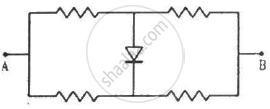
Each of the resistance shown in figure has a value of 20 Ω. Find the equivalent resistance between A and B. Does it depend on whether the point A or B is at higher potential?
What are the readings of the ammeters A1 and A2 shown in figure. Neglect the resistance of the meters.
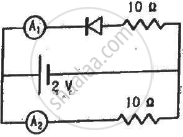
(Assume that the resistance of each diode is zero in forward bias and is infinity in reverse bias.)
A load resistor of 2kΩ is connected in the collector branch of an amplifier circuit using a transistor in common-emitter mode. The current gain β = 50. The input resistance of the transistor is 0.50 kΩ. If the input current is changed by 50µA. (a) by what amount does the output voltage change, (b) by what amount does the input voltage change and (c) what is the power gain?
Answer in detail.
Discuss the effect of external voltage on the width of depletion region of a p-n junction.
The depletion layer in the p-n junction diode is caused by ______.
p-n junction diode is formed
During the formation of a p-n junction ______.
