Advertisements
Advertisements
प्रश्न
Answer in detail.
Discuss the effect of external voltage on the width of depletion region of a p-n junction.
उत्तर
- A p-n junction can be connected to an external voltage supply in two possible ways.
- A p-n junction is said to be connected in a forward bias when the p-region connected to the positive terminal and the n-region is connected to the negative terminal of an external voltage source.
- In forward bias connection, the external voltage effectively opposes the built-in potential of the junction. The width of the depletion region is thus reduced.
- The second possibility of connecting the p-n junction is in a reverse-biased electric circuit.
- In reverse bias connection, the p-region is connected to the negative terminal and the n-region is connected to the positive terminal of the external voltage source. This external voltage effectively adds to the built-in potential of the junction. The width of the potential barrier is thus increased.
APPEARS IN
संबंधित प्रश्न
Write the two processes that take place in the formation of a p-n junction.
Explain briefly with the help of necessary diagrams, the reverse biasing of a p-n junction diode. Also draw characteristic curves.
Explain, with the help of a circuit diagram, the working of a photo-diode. Write briefly how it is used to detect the optical signals.
Mention the important considerations required while fabricating a p-n junction diode to be used as a Light Emitting Diode (LED). What should be the order of band gap of an LED if it is required to emit light in the visible range?
How is a zener diode fabricated so as to make it a special purpose diode? Draw I-V characteristics of zener diode and explain the significance of breakdown voltage.
Explain briefly, with the help of a circuit diagram, how a p-n junction diode works as a half wave rectifier.
When a p-type impurity is doped in a semiconductor, a large number of holes are created, This does not make the semiconductor charged. But when holes diffuse from the p-side to the n-side in a p-n junction, the n-side gets positively charged. Explain.
If the two ends of a p-n junction are joined by a wire,
The drift current in a p-n junction is
The diffusion current in a p-n junction is
A hole diffuses from the p-side to the n-side in a p-n junction. This means that
A semiconducting device is connected in a series circuit with a battery and a resistance. A current is found to pass through the circuit. If the polarity of the battery is reversed, the current drops to almost zero. the device may be
(a) an intrinsic semiconductor
(b) a p-type semiconductor
(c) an n-type semiconductor
(d) a p-n junction
The potential barrier existing across an unbiased p-n junction is 0.2 volt. What minimum kinetic energy a hole should have to diffuse from the p-side to the n-side if (a) the junction is unbiased, (b) the junction is forward-biased at 0.1 volt and (c) the junction is reverse-biased at 0.1 volt?
Consider a p-n junction diode having the characteristic \[i - i_0 ( e^{eV/kT} - 1) \text{ where } i_0 = 20\mu A\] . The diode is operated at T = 300 K . (a) Find the current through the diode when a voltage of 300 mV is applied across it in forward bias. (b) At what voltage does the current double?
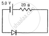
Calculate the current through the circuit and the potential difference across the diode shown in figure. The drift current for the diode is 20 µA.
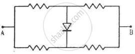
Each of the resistance shown in figure has a value of 20 Ω. Find the equivalent resistance between A and B. Does it depend on whether the point A or B is at higher potential?
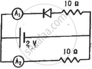
What are the readings of the ammeters A1 and A2 shown in figure. Neglect the resistance of the meters.
(Assume that the resistance of each diode is zero in forward bias and is infinity in reverse bias.)
Find the current through the battery in each of the circuits shown in figure.
(Assume that the resistance of each diode is zero in forward bias and is infinity in reverse bias.)
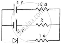
Find the current through the resistance R in figure if (a) R = 12Ω (b) R = 48Ω.
(Assume that the resistance of each diode is zero in forward bias and is infinity in reverse bias.)
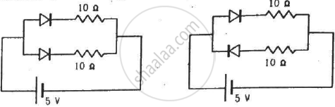
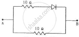
Find the equivalent resistance of the network shown in figure between the points A and B.
(Assume that the resistance of each diode is zero in forward bias and is infinity in reverse bias.)
When the base current in a transistor is changed from 30µA to 80µA, the collector current is changed from 1.0 mA to 3.5 mA. Find the current gain β.
A load resistor of 2kΩ is connected in the collector branch of an amplifier circuit using a transistor in common-emitter mode. The current gain β = 50. The input resistance of the transistor is 0.50 kΩ. If the input current is changed by 50µA. (a) by what amount does the output voltage change, (b) by what amount does the input voltage change and (c) what is the power gain?
Choose the correct option.
Current through a reverse-biased p-n junction increases abruptly at:
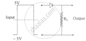
If in a p-n junction diode, a square input signal of 10 V is applied as shown Then the output signal across RL will be ______
Zener breakdown occurs in a p-n junction having p and n both:
The formation of the depletion region in a p-n junction diode is due to ______.
