Advertisements
Advertisements
प्रश्न
Find the current through the battery in each of the circuits shown in figure.
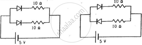
(Assume that the resistance of each diode is zero in forward bias and is infinity in reverse bias.)
उत्तर
We know that when a diode is forward biassed, it has zero resistance ideally. So, it can be replaced by a short circuit. When a diode is reverse biassed, it has infinite resistance ideally. So, it can be replaced by an open circuit.
(a) In the given circuit diagram, both diodes are forward biassed. So, the resistance of both of them is zero. Thus, the diode resistance is zero.
\[i = \frac{5}{\frac{10 \times 10}{10 + 10}} = \frac{5}{5} = 1 A\]
(b) One diode is forward biassed and the other is reverse biassed. The reverse-biassed diode is replaced by an open circuit, so no current flows through this branch.
The current passes through the forward-biassed diode only.
\[i = \frac{V}{R_{net}} = \frac{5}{10} = 0 . 5 A\]
APPEARS IN
संबंधित प्रश्न
In an unbiased p-n junction, holes diffuse from the p-region to n-region because ______.
In a p-n junction diode, the current I can be expressed as
I = `"I"_0 exp ("eV"/(2"k"_"BT") - 1)`
where I0 is called the reverse saturation current, V is the voltage across the diode and is positive for forward bias and negative for reverse bias, and I is the current through the diode, kBis the Boltzmann constant (8.6×10⁻⁵ eV/K) and T is the absolute temperature. If for a given diode I0 = 5 × 10⁻¹² A and T = 300 K, then
(a) What will be the forward current at a forward voltage of 0.6 V?
(b) What will be the increase in the current if the voltage across the diode is increased to 0.7 V?
(c) What is the dynamic resistance?
(d) What will be the current if reverse bias voltage changes from 1 V to 2 V?
Explain briefly with the help of necessary diagrams, the reverse biasing of a p-n junction diode. Also draw characteristic curves.
Explain, with the help of a circuit diagram, the working of a photo-diode. Write briefly how it is used to detect the optical signals.
Mention the important considerations required while fabricating a p-n junction diode to be used as a Light Emitting Diode (LED). What should be the order of band gap of an LED if it is required to emit light in the visible range?
Explain, with the help of a circuit diagram, the working of n-p-n transistor as a common emitter amplifier.
When a p-type impurity is doped in a semiconductor, a large number of holes are created, This does not make the semiconductor charged. But when holes diffuse from the p-side to the n-side in a p-n junction, the n-side gets positively charged. Explain.
If the two ends of a p-n junction are joined by a wire,
The diffusion current in a p-n junction is
Diffusion current in a p-n junction is greater than the drift current in magnitude
Two identical p-n junction may be connected in series with a battery in three ways. The potential difference across the two p-n junctions are equal in
In a p-n junction, a potential barrier of 250 meV exists across the junction. A hole with a kinetic energy of 300 meV approaches the junction. Find the kinetic energy of the hole when it crosses the junction if the hole approached the junction (a) from the p-side and (b) from the n-side.
Consider a p-n junction diode having the characteristic \[i - i_0 ( e^{eV/kT} - 1) \text{ where } i_0 = 20\mu A\] . The diode is operated at T = 300 K . (a) Find the current through the diode when a voltage of 300 mV is applied across it in forward bias. (b) At what voltage does the current double?
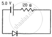
Calculate the current through the circuit and the potential difference across the diode shown in figure. The drift current for the diode is 20 µA.
What are the readings of the ammeters A1 and A2 shown in figure. Neglect the resistance of the meters.
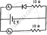
(Assume that the resistance of each diode is zero in forward bias and is infinity in reverse bias.)
Find the current through the resistance R in figure if (a) R = 12Ω (b) R = 48Ω.
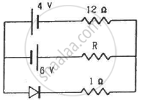
(Assume that the resistance of each diode is zero in forward bias and is infinity in reverse bias.)
The depletion layer in the p-n junction diode is caused by ______.
In a semiconductor diode, the barrier potential offers opposition to only ______.
p-n junction diode is formed
