Advertisements
Advertisements
प्रश्न
The formation of the depletion region in a p-n junction diode is due to ______.
विकल्प
movement of dopant atoms
diffusion of both electrons and holes
drift of electrons only
the drift of holes only
उत्तर
The formation of the depletion region in a p-n junction diode is due to the diffusion of both electrons and holes.
Explanation:
Charge diffusion is what creates the depletion area. holes diffuse across the junction from the p-side to the n-side due to the concentration gradient, whereas electrons diffuse from the n-side to the p-side. Near the junction, the holes and the electrons that are diffusely moving in the same direction unite.
APPEARS IN
संबंधित प्रश्न
Explain briefly with the help of necessary diagrams, the reverse biasing of a p-n junction diode. Also draw characteristic curves.
How is a zener diode fabricated so as to make it a special purpose diode? Draw I-V characteristics of zener diode and explain the significance of breakdown voltage.
Explain briefly, with the help of a circuit diagram, how a p-n junction diode works as a half wave rectifier.
In a p-n junction with open ends,
(a) there is no systematic motion of charge carries
(b) holes and conduction electrons systematically go from the p-side to n-side and from the n-side to p-side respectively
(c) there is no net charge transfer between the two sides
(d) there is a constant electric field near the junction.
When a p-n junction is reverse-biased, the current becomes almost constant at 25 µA. When it is forward-biased at 200 mV, a current of 75 µA is obtained. Find the magnitude of diffusion current when the diode is
(a) unbiased,
(b) reverse-biased at 200 mV and
(c) forward-biased at 200 mV.
Consider a p-n junction diode having the characteristic \[i - i_0 ( e^{eV/kT} - 1) \text{ where } i_0 = 20\mu A\] . The diode is operated at T = 300 K . (a) Find the current through the diode when a voltage of 300 mV is applied across it in forward bias. (b) At what voltage does the current double?
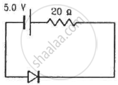
Calculate the current through the circuit and the potential difference across the diode shown in figure. The drift current for the diode is 20 µA.
Find the current through the battery in each of the circuits shown in figure.
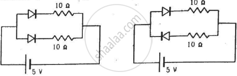
(Assume that the resistance of each diode is zero in forward bias and is infinity in reverse bias.)
A diode, a resistor and a 50 Hz AC source are connected in series. The number of current pulses per second through the resistor is __________ .
Answer in detail.
Discuss the effect of external voltage on the width of depletion region of a p-n junction.
In a semiconductor diode, the barrier potential offers opposition to only ______.
