Advertisements
Advertisements
Question
The formation of the depletion region in a p-n junction diode is due to ______.
Options
movement of dopant atoms
diffusion of both electrons and holes
drift of electrons only
the drift of holes only
Solution
The formation of the depletion region in a p-n junction diode is due to the diffusion of both electrons and holes.
Explanation:
Charge diffusion is what creates the depletion area. holes diffuse across the junction from the p-side to the n-side due to the concentration gradient, whereas electrons diffuse from the n-side to the p-side. Near the junction, the holes and the electrons that are diffusely moving in the same direction unite.
APPEARS IN
RELATED QUESTIONS
In a p-n junction diode, the current I can be expressed as
I = `"I"_0 exp ("eV"/(2"k"_"BT") - 1)`
where I0 is called the reverse saturation current, V is the voltage across the diode and is positive for forward bias and negative for reverse bias, and I is the current through the diode, kBis the Boltzmann constant (8.6×10⁻⁵ eV/K) and T is the absolute temperature. If for a given diode I0 = 5 × 10⁻¹² A and T = 300 K, then
(a) What will be the forward current at a forward voltage of 0.6 V?
(b) What will be the increase in the current if the voltage across the diode is increased to 0.7 V?
(c) What is the dynamic resistance?
(d) What will be the current if reverse bias voltage changes from 1 V to 2 V?
A student wants to use two p-n junction diodes to convert alternating current into direct current. Draw the labelled circuit diagram she would use and explain how it works.
The drift current in a p-n junction is 20.0 µA. Estimate the number of electrons crossing a cross section per second in the depletion region.
The current−voltage characteristic of an ideal p-n junction diode is given by \[i = i_0 ( e^{eV/KT} - 1)\] where, the drift current i0 equals 10 µA. Take the temperature T to be 300 K. (a) Find the voltage V0 for which \[e^{eV/kT} = 100 .\]One can neglect the term 1 for voltages greater than this value. (b) Find an expression for the dynamic resistance of the diode as a function of V for V > V0. (c) Find the voltage for which the dynamic resistance is 0.2 Ω.
(Use Planck constant h = 4.14 × 10⁻¹⁵ eV-s, Boltzmann constant k = 8·62 × 10-5 eV/K.)
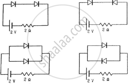
Find the currents through the resistance in the circuits shown in figure.

(Assume that the resistance of each diode is zero in forward bias and is infinity in reverse bias.)
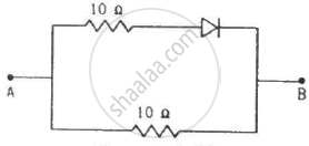
Draw the current-voltage characteristics for the device show in figure between the terminals A and B.

(Assume that the resistance of each diode is zero in forward bias and is infinity in reverse bias.)
Find the equivalent resistance of the network shown in figure between the points A and B.

(Assume that the resistance of each diode is zero in forward bias and is infinity in reverse bias.)
An AC source is connected to a diode and a resistor in series. Is the current thorough the resistor AC or DC?
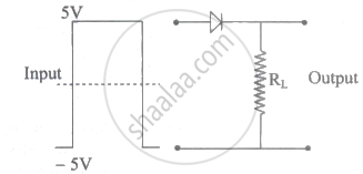
If in a p-n junction diode, a square input signal of 10 V is applied as shown Then the output signal across RL will be ______

Zener breakdown occurs in a p-n junction having p and n both:
