Advertisements
Advertisements
Question
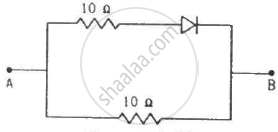
Draw the current-voltage characteristics for the device show in figure between the terminals A and B.
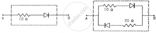
(Assume that the resistance of each diode is zero in forward bias and is infinity in reverse bias.)
Solution
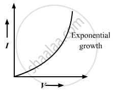
(a) If a battery is connected between terminals A and B, with positive terminal connected to point A and negative terminal connected to point B, then the diode will get forward biassed by the applied voltage. So, the current voltage graph for this circuit will be the same as that of the characteristic curves of a forward-biassed diode.
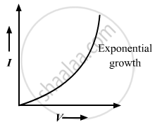
(b) If a battery is connected between terminals A and B, with positive terminal connected to point A and negative terminal connected to point B, then the upper diode will get forward biassed and the lower diode will get reverse biassed by the applied voltage. So, this lower branch can be replaced by an open circuit; hence, the current flow through this branch will be zero. The current flows only through the upper diode, so the circuit on simplification will become identical to the circuit in part (a). Hence, the current voltage graph for this circuit will be the same as that of the characteristic curves of a forward-biassed diode.
APPEARS IN
RELATED QUESTIONS
In an unbiased p-n junction, holes diffuse from the p-region to n-region because ______.
Write the two processes that take place in the formation of a p-n junction.
A zener diode is fabricated by heavily doping both p- and n- sides of the junction. Explain, why?
Mention the important considerations required while fabricating a p-n junction diode to be used as a Light Emitting Diode (LED). What should be the order of band gap of an LED if it is required to emit light in the visible range?
Draw a circuit diagram to study the input and output characteristics of an n-p-n transistor in its common emitter configuration. Draw the typical input and output characteristics.
How is a zener diode fabricated so as to make it a special purpose diode? Draw I-V characteristics of zener diode and explain the significance of breakdown voltage.
Explain briefly, with the help of a circuit diagram, how a p-n junction diode works as a half wave rectifier.
When a p-type impurity is doped in a semiconductor, a large number of holes are created, This does not make the semiconductor charged. But when holes diffuse from the p-side to the n-side in a p-n junction, the n-side gets positively charged. Explain.
The drift current in a reverse-biased p-n junction is increased in magnitude if the temperature of the junction is increased. Explain this on the basis of creation of hole-electron pairs.
Diffusion current in a p-n junction is greater than the drift current in magnitude
A hole diffuses from the p-side to the n-side in a p-n junction. This means that
The potential barrier existing across an unbiased p-n junction is 0.2 volt. What minimum kinetic energy a hole should have to diffuse from the p-side to the n-side if (a) the junction is unbiased, (b) the junction is forward-biased at 0.1 volt and (c) the junction is reverse-biased at 0.1 volt?
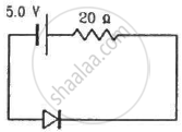
Calculate the current through the circuit and the potential difference across the diode shown in figure. The drift current for the diode is 20 µA.
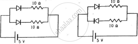
Find the currents through the resistance in the circuits shown in figure.
(Assume that the resistance of each diode is zero in forward bias and is infinity in reverse bias.)
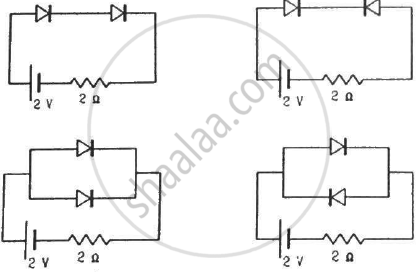
Find the current through the battery in each of the circuits shown in figure.
(Assume that the resistance of each diode is zero in forward bias and is infinity in reverse bias.)
Find the equivalent resistance of the network shown in figure between the points A and B.
(Assume that the resistance of each diode is zero in forward bias and is infinity in reverse bias.)
A diode, a resistor and a 50 Hz AC source are connected in series. The number of current pulses per second through the resistor is __________ .
Zener breakdown occurs in a p-n junction having p and n both:
The formation of the depletion region in a p-n junction diode is due to ______.
