Advertisements
Advertisements
Question
When a p-type impurity is doped in a semiconductor, a large number of holes are created, This does not make the semiconductor charged. But when holes diffuse from the p-side to the n-side in a p-n junction, the n-side gets positively charged. Explain.
Solution
A p-type semiconductor is formed by doping a group 13 element with group 14 element (Si or Ge). As the group 13 element has only 3 electrons in its valence shell and the group 14 element has 4 electrons in its valence shell, when the group 13 element, say, Al, replaces one Si in the silicon crystal, only 3 covalent bonds are formed by it. And the fourth covalent bond is left in need of one electron. So, it creates a hole. Since the atom as a whole is electriclly neutral, the p-type semiconductor is also neutral.
In a p‒n junction, when the diffusion of holes takes place across the junction because of the difference in the concentration of charge carriers from p to n sides, these holes neutralise some of the electrons on the n side. So, the atom attached with that electron becomes one electron deficient and hence positively charged. This makes the n side of the p‒n junction positively charged and the p side of the p‒n junction negatively charged.
APPEARS IN
RELATED QUESTIONS
In a p-n junction diode, the current I can be expressed as
I = `"I"_0 exp ("eV"/(2"k"_"BT") - 1)`
where I0 is called the reverse saturation current, V is the voltage across the diode and is positive for forward bias and negative for reverse bias, and I is the current through the diode, kBis the Boltzmann constant (8.6×10⁻⁵ eV/K) and T is the absolute temperature. If for a given diode I0 = 5 × 10⁻¹² A and T = 300 K, then
(a) What will be the forward current at a forward voltage of 0.6 V?
(b) What will be the increase in the current if the voltage across the diode is increased to 0.7 V?
(c) What is the dynamic resistance?
(d) What will be the current if reverse bias voltage changes from 1 V to 2 V?
A zener diode is fabricated by heavily doping both p- and n- sides of the junction. Explain, why?
The drift current in a reverse-biased p-n junction is increased in magnitude if the temperature of the junction is increased. Explain this on the basis of creation of hole-electron pairs.
If the two ends of a p-n junction are joined by a wire,
The diffusion current in a p-n junction is
In a p.n junction, the depletion region is 400 nm wide and an electric field of 5 × 10⁵ V m−1 exists in it. (a) Find the height of the potential barrier. (b) What should be the minimum kinetic energy of a conduction electron which can diffuse from the n-side to the p-side?
The potential barrier existing across an unbiased p-n junction is 0.2 volt. What minimum kinetic energy a hole should have to diffuse from the p-side to the n-side if (a) the junction is unbiased, (b) the junction is forward-biased at 0.1 volt and (c) the junction is reverse-biased at 0.1 volt?
The drift current in a p-n junction is 20.0 µA. Estimate the number of electrons crossing a cross section per second in the depletion region.
The current−voltage characteristic of an ideal p-n junction diode is given by \[i = i_0 ( e^{eV/KT} - 1)\] where, the drift current i0 equals 10 µA. Take the temperature T to be 300 K. (a) Find the voltage V0 for which \[e^{eV/kT} = 100 .\]One can neglect the term 1 for voltages greater than this value. (b) Find an expression for the dynamic resistance of the diode as a function of V for V > V0. (c) Find the voltage for which the dynamic resistance is 0.2 Ω.
(Use Planck constant h = 4.14 × 10⁻¹⁵ eV-s, Boltzmann constant k = 8·62 × 10-5 eV/K.)
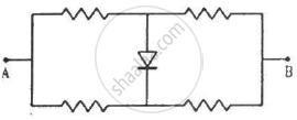
Each of the resistance shown in figure has a value of 20 Ω. Find the equivalent resistance between A and B. Does it depend on whether the point A or B is at higher potential?
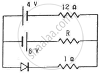
Find the current through the resistance R in figure if (a) R = 12Ω (b) R = 48Ω.
(Assume that the resistance of each diode is zero in forward bias and is infinity in reverse bias.)
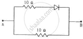
Find the equivalent resistance of the network shown in figure between the points A and B.
(Assume that the resistance of each diode is zero in forward bias and is infinity in reverse bias.)
When the base current in a transistor is changed from 30µA to 80µA, the collector current is changed from 1.0 mA to 3.5 mA. Find the current gain β.
A load resistor of 2kΩ is connected in the collector branch of an amplifier circuit using a transistor in common-emitter mode. The current gain β = 50. The input resistance of the transistor is 0.50 kΩ. If the input current is changed by 50µA. (a) by what amount does the output voltage change, (b) by what amount does the input voltage change and (c) what is the power gain?
Answer in detail.
Discuss the effect of external voltage on the width of depletion region of a p-n junction.
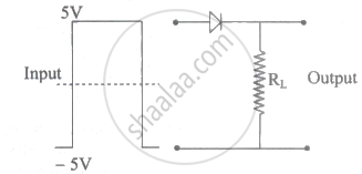
If in a p-n junction diode, a square input signal of 10 V is applied as shown Then the output signal across RL will be ______
p-n junction diode is formed
The formation of the depletion region in a p-n junction diode is due to ______.
