Advertisements
Advertisements
Question
Draw separate energy band diagram for conductors, semiconductors and insulators and
label each of them.
Solution
Energy Band Diagrams
Conductors
Here conduction Band and valance Band are partly overlapped

Insulators
Here forbidden gap is large between conduction Band and Valance Band

Semiconductors
Here forbidden gap is less than 1 eV

APPEARS IN
RELATED QUESTIONS
Distinguish between a metal and an insulator on the basis of energy band diagrams ?
Distinguish between a conductor, a semiconductor and an insulator on the basis of energy band diagrams.
There are energy bands in a solid. Do we have really continuous energy variation in a band ro do we have very closely spaced but still discrete energy levels?
Electric conduction in a semiconductor takes place due to
When an impurity is doped into an intrinsic semiconductor, the conductivity of the semiconductor
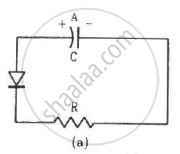
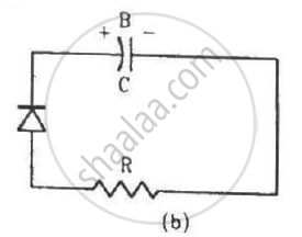
Two identical capacitors A and B are charged to the same potential V and are connected in two circuits at t = 0 as shown in figure. The charges on the capacitors at a time t = CRare, respectively,


An incomplete sentence about transistors is given below:
The emitter−..... junction is __ and the collector−..... junction is __. The appropriate words for the dotted empty positions are, respectively,
In a pure semiconductor, the number of conduction election 6 × 10¹⁹ per cubic metre. How many holes are there in a sample of size 1 cm × 1 mm?
What is forbidden band?
In a common base configuration Ie = 1 mA α = 0.95 the value of base current is
