Advertisements
Advertisements
Question
How does the doping increase the conductivity of semiconductors?
Solution
For pratical use conductivity of a semiconductor is very low conductivity can be increased by adding small impurity, this process is called doping. Doping can be done with an impurity which ie electron rich or electron deficient.
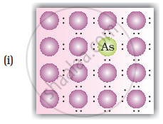
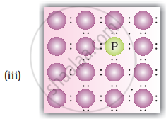
• n-type semiconductors: Silicion or Germanium (group - 14) doped with electron rich impurity (group - 15 element like P or As) is called n-tyoe semiconductors. Here conductivity is due to the extra electron or delocalized electron.
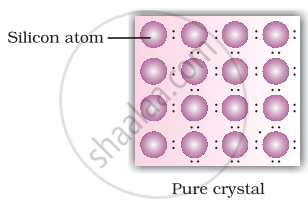
Explanation for increase in conductivity in n-type semiconductors: When intrinsic semiconductors like Si or Ge are doped with pentavalent elements as P or As, they occupy some of the lattice sites in silicon or germanium crystal. Four out of five electrons are used in formation of four covalent bonds with neighbouring silicion atoms. The fifth electron is extra and gets delocalised. These delocalised electrons increase the conductivity of doped silicion (or germainium)
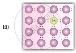
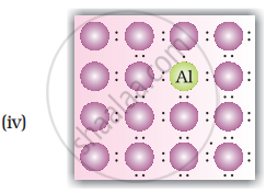
• p-type semiconductors: Silicion or Germanium (group - 14) doped with electron deficient impurity (group 13 element like B or Al or Ga) is called p-type semiconductors. HEre conductivity is due to positively charged electron holes.
Explanation for increase in conductivity in p-type semiconductors: In this case the doping of intrinsic semiconductors like silicion or germanium with trivalent elements like B/In/Ga, three out of four electrons in silicion or germanium form bonds with doping impurity (i.e. B/In/Ga). The fourth electron remains unbonded. The place where fourth valence electron is missing is called electron hole or electron vacancy. An electron from neighbouring atom can come and fill up the lectron hole, but in doing so it would leave an electron hole at its original position. If this happens it would appear that electron hole has moved in a direction opposite to that of the electron that filled it. Under the influence of electric field electrons would move towards the positively charged plate through electron holes, but it would appear as if electrons are positively charged and are moving towards the negatively charged plate.
APPEARS IN
RELATED QUESTIONS
p - type semi-conductors are made by mixing silicon with impurities of-
- germanium
- boron
- arsenic
- antimony
What type of semiconductor is obtained when silicon is doped with boron?
When a hole is produced in P-type semiconductor, there is _______.
Give reasons : Silicon on doping with Phosphorous forms n-type semiconductor.
Distinguish between p-type and n-type semiconductors.
A group of 14 elements is converted into n-type semiconductor by doping it with:
Group 14 element is converted to p-type semiconductor by doping it with:
p-type semiconductors are formed when Si or Ge are doped with ____________.
Under the influence of electric field, which of the following statements is true about the movement of electrons and holes in a p-type semiconductor?
(i) Electron will move towards the positvely charged plate through electron holes.
(ii) Holes will appear to be moving towards the negatively charged plate.
(iii) Both electrons and holes appear to move towards the positively charged plate.
(iv) Movement of electrons is not related to the movement of holes.
A perfect crystal of silicon (Figure) is doped with some elements as given in the options. Which of these options show n-type semiconductors?