Advertisements
Advertisements
प्रश्न
We have valence electrons and conduction electrons in a semiconductor. Do we also have 'valence holes' and 'conduction holes'?
उत्तर
Holes do not exist in reality. They exist only virtually. When an electron jumps from the valence band to the conduction band, a vacancy is created at the place from where the electron had jumped. This vacancy is called a hole. So, a valence or conduction hole is a virtual concept only.
APPEARS IN
संबंधित प्रश्न
Distinguish between a conductor and a semi conductor on the basis of energy band diagram
How many 1s energy states are present in one mole of sodium vapour? Are they all filled in normal conditions? How many 3s energy states are present in one mole of sodium vapour? Are they all filled in normal conditions?
In semiconductors, thermal collisions are responsible for taking a valence electron to the conduction band. Why does the number of conduction electrons not go on increasing with time as thermal collisions continuously take place?
An electric field is applied to a semiconductor. Let the number of charge carries be nand the average drift speed by v. If the temperature is increased,
A p-type semiconductor is
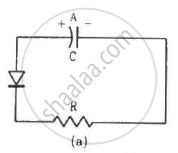
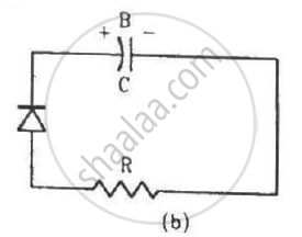
Two identical capacitors A and B are charged to the same potential V and are connected in two circuits at t = 0 as shown in figure. The charges on the capacitors at a time t = CRare, respectively,


In a transistor,
The impurity atoms with which pure silicon may be doped to make it a p-type semiconductor are those of
(a) phosphorus
(b) boron
(c) antimony
(d) aluminium.
Indium antimonide has a band gap of 0.23 eV between the valence and the conduction band. Find the temperature at which kT equals the band gap.
Let ΔE denote the energy gap between the valence band and the conduction band. The population of conduction electrons (and of the holes) is roughly proportional to e−ΔE/2kT. Find the ratio of the concentration of conduction electrons in diamond to the in silicon at room temperature 300 K. ΔE for silicon is 1.1 eV and for diamond is 6.1 eV. How many conduction electrons are likely to be in one cubic metre of diamond?
Estimate the proportion of boron impurity which will increase the conductivity of a pure silicon sample by a factor of 100. Assume that each boron atom creates a hole and the concentration of holes in pure silicon at the same temperature is 7 × 10¹⁵ holes per cubic metre. Density of silicon 5 × 1028 atoms per cubic metre.
The product of the hole concentration and the conduction electron concentration turns out to be independent of the amount of any impurity doped. The concentration of conduction electrons in germanium is 6 × 10¹⁹ per cubic metref conduction electrons increases to 2 × 10²³ per cubic metre. Find the concentration of the holes in the doped germanium.. When some phosphorus impurity is doped into a germanium sample, the concentration o
What is forbidden band?
An n-type semiconductor is
In a semiconductor, the forbidden energy gap between the valence, band and the conduction band is of the order of
In a common base configuration Ie = 1 mA α = 0.95 the value of base current is
- Assertion (A): In insulators, the forbidden gap is very large.
- Reason (R): The valence electrons in an atom of an insulator are very tightly bound to the nucleus.
Which one of the following elements will require the highest energy to take out an electron from them?
Pb, Ge, C and Si
