Advertisements
Advertisements
प्रश्न
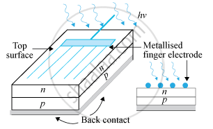
What is a solar cell?
उत्तर
It is a semiconductor device used to convert photons of solar light into electricity. It generates emf when solar radiation falls on the p-n junction. A p-type silicon wafer of about 300 μm is taken over which a thin layer of n-type silicon is grown on one side by the diffusion process.

APPEARS IN
संबंधित प्रश्न
If a small voltage is applied to a p-n junction diode, how will the barrier potential be affected when it is(ii) reveres biased?
With what considerations in view, a photodiode is fabricated? State its working with the help of a suitable diagram.
Even though the current in the forward bias is known to be more than in the reverse bias, yet the photodiode works in reverse bias. What is the reason?
Using the necessary circuit diagrams, show how the V-I characteristics of a p-n junction are obtained in
Reverse biasing
How are these characteristics made use of in rectification?
Why is zener diode fabricated by heavily doping both p- and n-sides of the junction?
Briefly explain its working. Draw its V - I characteristics for two different intensities of illumination ?
What happens to the width of depletion player of a p-n junction when it is (i) forward biased, (ii) reverse biased?
Explain the formation of depletion layer and potential barrier in a p−n junction.
An ideal diode should pass a current freely in one direction and should stop it completely in the opposite direction. Which is closer to ideal-vacuum diode or a p-njunction diode?
Pressure P varies as P = `alpha/beta "exp" (- (alpha x)/"k"_"BT")`, where x denotes the distance, kB is the Boltzmann's constant, T is the absolute temperature and α and β are constant. The dimension of β is ______.
Consider the following statements (A) and (B) and identify the correct answer.
- A Zener diode is connected in reverse bias when used as a voltage regulator.
- The potential barrier of the p-n junction lies between 0.1 V to 0.3 V.
