Advertisements
Advertisements
Question
Explain briefly with the help of necessary diagrams, the forward biasing of a p-n junction diode. Also draw characteristic curves.
Solution
p-n junction diode under forward bias

p-side is connected to positive terminal and n-side to the negative terminal.
Applied voltage drops across the depletion region.
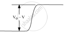
Direction of applied voltage (V) is opposite to the build in potential (V0).
As the depletion layer width decreases, the barrier height is reduced.
Effective barrier height under forward bias is (V0 − V).
-
Electron in n-region moves towards the p-n junction and holes in p-region move towards the junction. The width of the depletion layer decreases and hence, it offers less resistance.
-
Diffusion of majority carriers takes place across the junction.
This leads to forward current.
APPEARS IN
RELATED QUESTIONS
In a p-n junction diode, the current I can be expressed as
I = `"I"_0 exp ("eV"/(2"k"_"BT") - 1)`
where I0 is called the reverse saturation current, V is the voltage across the diode and is positive for forward bias and negative for reverse bias, and I is the current through the diode, kBis the Boltzmann constant (8.6×10⁻⁵ eV/K) and T is the absolute temperature. If for a given diode I0 = 5 × 10⁻¹² A and T = 300 K, then
(a) What will be the forward current at a forward voltage of 0.6 V?
(b) What will be the increase in the current if the voltage across the diode is increased to 0.7 V?
(c) What is the dynamic resistance?
(d) What will be the current if reverse bias voltage changes from 1 V to 2 V?
A student wants to use two p-n junction diodes to convert alternating current into direct current. Draw the labelled circuit diagram she would use and explain how it works.
Explain, with the help of a circuit diagram, the working of n-p-n transistor as a common emitter amplifier.
If the two ends of a p-n junction are joined by a wire,
In a p-n junction,
(a) new holes and conduction electrons are produced continuously throughout the material
(b) new holes and conduction electrons are produced continuously throughout the material except in the depletion region
(c) holes and conduction electrons recombine continuously throughout the material
(d) holes and conduction electrons recombine continuously throughout the material except in the depletion region.
Consider a p-n junction diode having the characteristic \[i - i_0 ( e^{eV/kT} - 1) \text{ where } i_0 = 20\mu A\] . The diode is operated at T = 300 K . (a) Find the current through the diode when a voltage of 300 mV is applied across it in forward bias. (b) At what voltage does the current double?
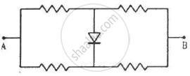
Each of the resistance shown in figure has a value of 20 Ω. Find the equivalent resistance between A and B. Does it depend on whether the point A or B is at higher potential?

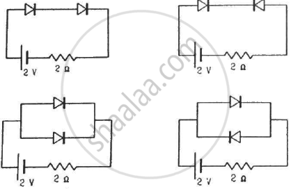
Find the currents through the resistance in the circuits shown in figure.

(Assume that the resistance of each diode is zero in forward bias and is infinity in reverse bias.)
Choose the correct option.
Current through a reverse-biased p-n junction increases abruptly at:
During the formation of a p-n junction ______.
