Advertisements
Advertisements
Question
Explain the formation of the barrier potential in a p-n junction.
Solution
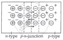
A p-n junction is formed by bringing p-type and n-type semiconductors together in very close proximity.
At the instant of p-n-junction, movement of free electrons from the n-side and free holes from the p-side diffuse across the junction and combine and thus leave -ve ions on the p-side and +ve ions inn-side.
These two layers of +ve and -ve ions form the depletion region and the potential difference thus sets up is called the potential barrier.
RELATED QUESTIONS
What causes the setting up of high electric field even for small reverse bias voltage across the diode?
In semiconductor physics, what is meant by:
(i) rectifier
(ii) an amplifier
(iii) an oscillator
Diffusion in a p-n junction is due to ______.
What are the applications of p - n Junction diode?
The nature of binding for a crystal with alternate and evenly spaced positive and negatively ions is
In a semiconductor diode, the barrier potential offers opposition to only
Consider an npn transistor with its base-emitter junction forward biased and collector base junction reverse biased. Which of the following statements are true?
- Electrons crossover from emitter to collector.
- Holes move from base to collector.
- Electrons move from emitter to base.
- Electrons from emitter move out of base without going to the collector.
A Zener of power rating 1 W is to be used as a voltage regulator. If zener has a breakdown of 5 V and it has to regulate voltage which fluctuated between 3 V and 7 V, what should be the value of Rs for safe operation (Figure)?

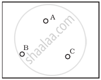
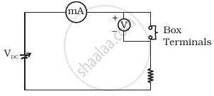
Consider a box with three terminals on top of it as shown in figure (a):
 (a) |
Three components namely, two germanium diodes and one resistor are connected across these three terminals in some arrangement. A student performs an experiment in which any two of these three terminals are connected in the circuit shown in figure (b).
 (b) |
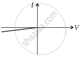
The student obtains graphs of current-voltage characteristics for unknown combination of components between the two terminals connected in the circuit. The graphs are
(i) when A is positive and B is negative
 (c) |
(ii) when A is negative and B is positive
 (d) |
(iii) When B is negative and C is positive
|
(e) |
(iv) When B is positive and C is negative
 (f) |
(v) When A is positive and C is negative
 (g) |
(vi) When A is negative and C is positive
 (h) |
From these graphs of current-voltage characteristics shown in figure (c) to (h), determine the arrangement of components between A, B and C.
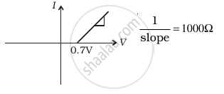
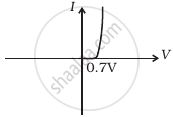
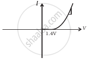
Draw V-I characteristics of a p-n Junction diode.
