Advertisements
Advertisements
Question
When a forward bias is applied to a p-n junction, it ______.
Options
raises the potential barrier.
reduces the majority carrier current to zero.
lowers the potential barrier.
None of the above.
Solution
When a forward bias is applied to a p-n junction, it lowers the potential barrier.
Explanation:
When a forward bias is applied to a p-n junction, it lowers the value of potential barrier. In the case of a forward bias, the potential barrier opposes the applied voltage. Hence, the potential barrier across the junction gets reduced.
APPEARS IN
RELATED QUESTIONS
Explain the working of P-N junction diode in forward and reverse biased mode.
What happens when a forward bias is applied to a p-n junction?
What causes the setting up of high electric field even for small reverse bias voltage across the diode?
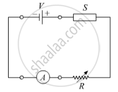
In the following diagram 'S' is a semiconductor. Would you increase or decrease the value of R to keep the reading of the ammeter A constant when S is heated? Give reason for your answer.

Draw its I – V characteristics of photodiode
What is the use of Zener diode?
With reference to a semiconductor diode, what is meant by:
(i) Forward bias
(ii) Reverse bias
(iii) Depletion region
Of the diodes shown in the following diagrams, which one is reverse biased?
A – pn junction has a depletion layer of thickness .of the order of
When we apply reverse biased to a junction diode, it
Use a transistor as an amplition
The expected energy of the electron at absolute zero is called:-
On increasing the reverse biases voltage to a large value in a P – N junction diode-current
The breakdown in a reverse biased p–n junction diode is more likely to occur due to ______.
- large velocity of the minority charge carriers if the doping concentration is small.
- large velocity of the minority charge carriers if the doping concentration is large.
- strong electric field in a depletion region if the doping concentration is small.
- strong electric field in the depletion region if the doping concentration is large.
A Zener of power rating 1 W is to be used as a voltage regulator. If zener has a breakdown of 5 V and it has to regulate voltage which fluctuated between 3 V and 7 V, what should be the value of Rs for safe operation (Figure)?

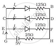
If each diode in figure has a forward bias resistance of 25 Ω and infinite resistance in reverse bias, what will be the values of the current I1, I2, I3 and I4?

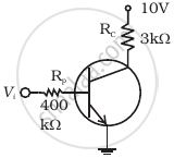
In the circuit shown in figure, when the input voltage of the base resistance is 10 V, Vbe is zero and Vce is also zero. Find the values of Ib, Ic and β.

Draw the circuit arrangement for studying V-I characteristics of a p-n junction diode in (i) forward biasing and (ii) reverse biasing. Draw the typical V-I characteristics of a silicon diode.
With reference to a semiconductor diode, define the depletion region.
Draw a labelled characteristic curve (l-V graph) for a semiconductor diode during forward bias.
