Advertisements
Advertisements
Question
Why is a zener diode considered as a special purpose semiconductor diode?
Solution
Zener diode works only in reverse breakdown region that’s why it in considered as a special purpose semiconductor.
RELATED QUESTIONS
What causes the setting up of high electric field even for small reverse bias voltage across the diode?
With reference to semiconductor devices, define a p-type semiconductor and a Zener diode.
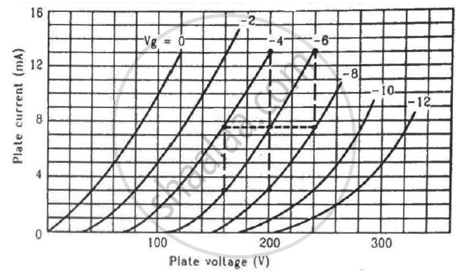
Find the values of rp, µ and gm of a triode operating at plate voltage 200 V and grid voltage −6. The plate characteristics are shown in the figure.

What are the applications of p - n Junction diode?
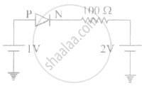
The current through an ideal PN-junction shown in the following circuit diagram will be:

When an electric field is applied across a semiconductor ______.
- electrons move from lower energy level to higher energy level in the conduction band.
- electrons move from higher energy level to lower energy level in the conduction band.
- holes in the valence band move from higher energy level to lower energy level.
- holes in the valence band move from lower energy level to higher energy level.
Consider an npn transistor with its base-emitter junction forward biased and collector base junction reverse biased. Which of the following statements are true?
- Electrons crossover from emitter to collector.
- Holes move from base to collector.
- Electrons move from emitter to base.
- Electrons from emitter move out of base without going to the collector.
 (a) |
 (b) |
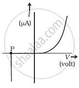
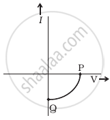
- Name the type of a diode whose characteristics are shown in figure (A) and figure (B).
- What does the point P in figure (A) represent?
- What does the points P and Q in figure (B) represent?
Draw a labelled characteristic curve (l-V graph) for a semiconductor diode during forward bias.
An ideal PN junction diode offers ______.
