Advertisements
Advertisements
प्रश्न
In a photo diode, the conductive increases when the material is exposed to light. It is found that the conductivity changes only if the wavelength is less than 620 nm. What is the band gap?
(Use Planck constant h = 4.14 × 10⁻¹⁵ eV-s, Boltzmann constant k = 8·62 × 10-5 eV/K.)
उत्तर
Conductivity of any material increases when the number of free charge carriers in the material increases. When a photo diode is exposed to light, additional electron hole pairs are created in the diode; thus, its conductivity increases. So to change the conductivity of a photo diode, the minimum energy of the incident radiation should be equal to the band gap of the material.
In other words,
Band gap = Energy of the incident radiation
\[\Rightarrow E = \frac{hc}{\lambda}\]
\[ \Rightarrow E = \frac{1242 \text{ eV - nm}}{620 \text{ nm }} = 2.0eV\]
APPEARS IN
संबंधित प्रश्न
(i) Explain with the help of a diagram the formation of depletion region and barrier potential in a pn junction.
When a forward bias is applied to a p-n junction, it ______.
What is the use of Zener diode?
Plot a graph showing variation of current versus voltage for the material GaAs ?
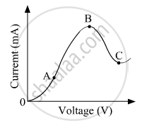
The graph shown in the figure represents a plot of current versus voltage for a given semiconductor. Identify the region, if any, over which the semiconductor has a negative resistance.
Show on a graph, the variation of resistivity with temperature for a typical semiconductor.
A triode value operates at Vp = 225 V and Vg = −0.5 V.
The plate current remains unchanged if the plate voltage is increased to 250 V and the grid voltage is decreased to −2.5 V. Calculate the amplification factor.
The dynamic plate resistance of a triode value is 10 kΩ. Find the change in the plate current if the plate voltage is changed from 200 V to 220 V.
Answer the following question.
Why photodiodes are required to operate in reverse bias? Explain.
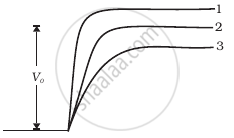
In Figure, Vo is the potential barrier across a p-n junction, when no battery is connected across the junction ______.
Can the potential barrier across a p-n junction be measured by simply connecting a voltmeter across the junction?
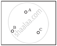
Consider a box with three terminals on top of it as shown in figure (a):
 (a) |
Three components namely, two germanium diodes and one resistor are connected across these three terminals in some arrangement. A student performs an experiment in which any two of these three terminals are connected in the circuit shown in figure (b).
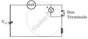 (b) |
The student obtains graphs of current-voltage characteristics for unknown combination of components between the two terminals connected in the circuit. The graphs are
(i) when A is positive and B is negative
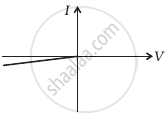 (c) |
(ii) when A is negative and B is positive
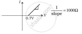 (d) |
(iii) When B is negative and C is positive
|
(e) |
(iv) When B is positive and C is negative
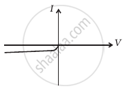 (f) |
(v) When A is positive and C is negative
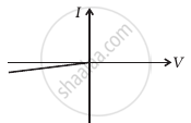 (g) |
(vi) When A is negative and C is positive
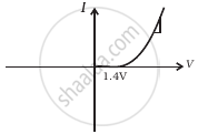 (h) |
From these graphs of current-voltage characteristics shown in figure (c) to (h), determine the arrangement of components between A, B and C.
Write the property of a junction diode which makes it suitable for rectification of ac voltages.
Explain the formation of the barrier potential in a p-n junction.
Answer the following giving reasons:
A p-n junction diode is damaged by a strong current.
A semiconductor device is connected in series with a battery, an ammeter and a resistor. A current flows in the circuit. If. the polarity of the battery is reversed, the current in the circuit almost becomes zero. The device is a/an ______.
Describe briefly the following term:
minority carrier injection in forward biasing.
What is meant by forward biasing of a semiconductor diode?
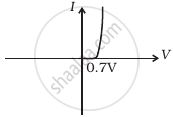
Draw a labelled characteristic curve (l-V graph) for a semiconductor diode during forward bias.
