Advertisements
Advertisements
Question
Draw the circuit symbol for NPN and PNP transistors. What is the difference in the Emitter, Base, and Collector regions of a transistor?
Solution
The circuit symbols of the two types of transistors:
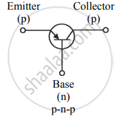
Figure (a)

Figure (b)
The difference in the Emitter (E), the Base (b), and the Collector (C) are as follows:
- Emitter: It is a thick heavily doped layer. This supplies a large number of majority carriers for the current flow through the transistor
- Base: It is the thin, lightly doped central layer.
- Collector: It is a thick and moderately doped layer. Its area is larger than that of the emitter and the base. This layer collects a major portion of the majority of carriers supplied by the emitter. The collector also helps dissipation of any small amount of heat generated.
APPEARS IN
RELATED QUESTIONS
Why are the emitter, the base, and the collector of a BJT doped differently?
Which method of biasing is used for operating a transistor as an amplifier?
In a transistor amplifier, IC = 5.5 mA , IE = 5.6 mA. The current amplification factor β is ______
Draw the circuit symbol of the PNP transistor.
Draw the circuit diagram to study the characteristic of the transistor in common emitter mode. Draw the input and output characteristics.
Transistor functions as a switch. Explain.
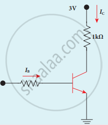
Assuming VCEsat = 0.2 V and β = 50, find the minimum base current (IB) required to drive the transistor given in the figure to saturation.
A transistor of α = 0.99 and VBE = 0.7 V is connected in the common-emitter configuration as shown in the figure. If the transistor is in the saturation region, find the value of collector current.
In a common emitter amplifier, the input resistance is 1000 Ω, the peak value of Input signal voltage is 5 mV, and β = 60. The peak value of output current is
Least doped region in a transistor ____________.
In the study of transistor as an amplifier, the ratio of collector current to emitter current is 0.98 then the ratio of collector current to base current will be ______.
In an npn transistor, the base current is 100 µA and the collector current is 10 mA. The emitter current is ______.
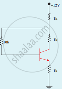
ln switching circuit, transistor is in ON state and values of IC and IB are 4.2 mA and 5 µA respectively and RC= l k`Omega` and RB= 300 k`Omega`. If VBE = 0.5 V, find the value of VBB.
In an npn transistor circuit, the collector current is 10 mA. If 90% of the electrons emitted reach the collector, the emitter current (IE) and base current (IB) are given by ____________.
In a transistor, a change of 8.0 mA in the emitter current produces a change of 7.8 mA in the collector current. Then change in the base current is ____________.
A pnp transistor is used in common-emitter mode. If a change of 40 µA in base current brings a change of 2 µA in collector current with 0.04 V in base-emitter voltage, then the input resistance is ____________.
In the case of transistor, the relation between current ratios αdc and βdc is ______.
In common emitter amplifier, a change of 0.2 mA in the base current causes a change of 5 mA in the collector current. If input resistance is 2K `Omega` and voltage gain is 75, the load resistance used in the circuit is ______.
In a study of transistor as an amplifier, the ratio of collector current to emitter current is 0.98. The collector current is 3mA, then base current will be approximately ______.
In the common-emitter configuration of a transistor, the current gain is more than 1 because [lb, le, and lc are base, emitter, and collector currents respectively] ______
For a transistor, αdc and βdc are the current ratios, then the value of `(beta_"dc"-delta_"dc")/(alpha_"dc".beta_"dc")`
The current amplification factor for a transistor in its common emitter mode is 50. The current amplification factor in the common base mode of the transistor is ______.
How is a transistor biased for operating it as amplifier?
Explain the output characteristics of common emitter configuration of n-p-n transistor.
Define β
