Advertisements
Advertisements
Question
Why are the emitter, the base, and the collector of a BJT doped differently?
Solution
A BJT is a bipolar device, both electrons and holes participate in the conduction process. Under the forward-biased condition, the majority of carriers injected from the emitter into the base constitute the largest current component in a BJT. For these carriers to diffuse across the base region with negligible recombination and reach the collector junction, they must overwhelm the majority of carriers of the opposite charge in the base. The total emitter current has two components, due to majority carriers in the emitter and due to minority carriers diffusing from the base into the emitter. The ratio of the current component due to the injected majority carriers from the emitter to the total emitter current is a measure of the emitter efficiency. To improve the emitter efficiency and the common-base current gain (α), it can be shown that the emitter should be much more heavily doped than the base.
Also, the base width is a function of the base-collector voltage. A low doping level of the collector increases the size of the depletion region. This increases the maximum collector-base voltage and reduces the base width. Further, the large depletion region at the collector-base junction-extending mainly into the collector-corresponds to a smaller electric field and avoids avalanche breakdown of the reverse-biased collector-base junction.
[Note: Effective dopant concentrations of (a) npn transistor (b) pnp transistor are shown below.]
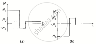
The base doping is less than the emitter doping but greater than the collector doping.
RELATED QUESTIONS
Why is the base of a transistor made thin and is lightly doped?
Derive the relation between α and β.
For a transistor β =75 and IE = 7.5 mA. The value of α is ______
In a transistor amplifier, IC = 5.5 mA , IE = 5.6 mA. The current amplification factor β is ______
Draw the circuit symbol for NPN and PNP transistors. What is the difference in the Emitter, Base, and Collector regions of a transistor?
The light emitted in an LED is due to
Sketch the static characteristics of a common emitter transistor and bring out the essential features of input and output characteristics.
Describe the function of a transistor as an amplifier with the neat circuit diagram. Sketch the input and output wave forms.
In the circuit shown in the figure, the BJT has a current gain (β) of 50. For an emitter-base voltage VEB = 600 mV, calculate the emitter-collector voltage VEC (in volts).
A transistor has a voltage gain A. If the amount βA of its output is applied to the input of the transistor, then the transistor becomes oscillator, when ______.
A common emitter amplifier is designed with n-p-n transistor (α = 0.99). The input impedance is 1 kΩ and the load is 10 kΩ. The voltage gain will be ______
The condition to convert an amplified signal into an oscillating signal is ______
For a transistor, the current ratio 'βdc' is defined as the ratio of ______.
In the symbol for a transistor, the arrow head points in the direction of the ____________.
In switching circuit, transistor is in ON state. Values of IC and IB are 5.2 mA and 10 µA respectively and value of RC is 1 k`Omega`. If Vcc is at 5.5 V, then VCE is ______.
In an npn transistor, the base current is 100 µA and the collector current is 10 mA. The emitter current is ______.
In an npn transistor, the collector current is 24 mA. If 80% of electrons reach collector, its base current in mA is ______.
In a silicon transistor, a change of 7.89 mA in the emitter current if produces a change of 7.8 mA in the collector current, then the base current must change by ____________.
In a transistor, a change of 8.0 mA in the emitter current produces a change of 7.8 mA in the collector current. Then change in the base current is ____________.
A transistor is connected in C - E mode. If collector current is 72 × 10-5 A and α = 0.96, then base current will be ______.
For an ideal diode, the current in the following arrangement is ______.
In the common-emitter configuration of a transistor, the current gain is more than 1 because [lb, le, and lc are base, emitter, and collector currents respectively] ______
A common emitter amplifier has a voltage gain of 50, an input impedance of 100Ω and an output impedance of 2000Ω. The power gain of the amplifier is ______.
For a transistor, αdc and βdc are the current ratios, then the value of `(beta_"dc"-delta_"dc")/(alpha_"dc".beta_"dc")`
The transfer ratio of a transistor is 50. The input resistance of the transistor when used in the CE configuration is 1K Ω. The peak value for an AC input voltage of 0.01 V of collector current is ______.
Explain the working of the n-p-n transistor in a common base configuration.
The collector current in a common-emitter transistor amplifier is 4 mA. When the base current is increased by 20 µA, the collector current increases to 6 mA. The current gain is ______.
