Advertisements
Advertisements
Question
In a p-n junction, a potential barrier of 250 meV exists across the junction. A hole with a kinetic energy of 300 meV approaches the junction. Find the kinetic energy of the hole when it crosses the junction if the hole approached the junction (a) from the p-side and (b) from the n-side.
Solution
Given:
Potential barrier, d = 250 meV
Initially,
Kinetic energy of a hole = 330 meV
We know that the kinetic energy of a hole decreases when the junction is forward biassed (because of the energy loss in crossing the junction).
Also, the kinetic energy of a hole increases when the junction is reverse biassed (because reverse bias voltage pushes the hole on the n-side towards the junction) in the given the p-n junction diode.
(a) The kinetic energy of a hole decreases under forward bias.
∴ Final kinetic energy = (300 − 250) meV
= 50 meV
(b) The kinetic energy of a hole increases under reverse bias.
∴ Final kinetic energy = (300 + 250) meV
= 550 meV
APPEARS IN
RELATED QUESTIONS
In an unbiased p-n junction, holes diffuse from the p-region to n-region because ______.
A zener diode is fabricated by heavily doping both p- and n- sides of the junction. Explain, why?
Explain briefly with the help of necessary diagrams, the forward biasing of a p-n junction diode. Also draw characteristic curves.
Explain, with the help of a circuit diagram, the working of a photo-diode. Write briefly how it is used to detect the optical signals.
Mention the important considerations required while fabricating a p-n junction diode to be used as a Light Emitting Diode (LED). What should be the order of band gap of an LED if it is required to emit light in the visible range?
When a p-type impurity is doped in a semiconductor, a large number of holes are created, This does not make the semiconductor charged. But when holes diffuse from the p-side to the n-side in a p-n junction, the n-side gets positively charged. Explain.
The drift current in a reverse-biased p-n junction is increased in magnitude if the temperature of the junction is increased. Explain this on the basis of creation of hole-electron pairs.
If the two ends of a p-n junction are joined by a wire,
In a p.n junction, the depletion region is 400 nm wide and an electric field of 5 × 10⁵ V m−1 exists in it. (a) Find the height of the potential barrier. (b) What should be the minimum kinetic energy of a conduction electron which can diffuse from the n-side to the p-side?
The current−voltage characteristic of an ideal p-n junction diode is given by \[i = i_0 ( e^{eV/KT} - 1)\] where, the drift current i0 equals 10 µA. Take the temperature T to be 300 K. (a) Find the voltage V0 for which \[e^{eV/kT} = 100 .\]One can neglect the term 1 for voltages greater than this value. (b) Find an expression for the dynamic resistance of the diode as a function of V for V > V0. (c) Find the voltage for which the dynamic resistance is 0.2 Ω.
(Use Planck constant h = 4.14 × 10⁻¹⁵ eV-s, Boltzmann constant k = 8·62 × 10-5 eV/K.)
Consider a p-n junction diode having the characteristic \[i - i_0 ( e^{eV/kT} - 1) \text{ where } i_0 = 20\mu A\] . The diode is operated at T = 300 K . (a) Find the current through the diode when a voltage of 300 mV is applied across it in forward bias. (b) At what voltage does the current double?
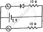
What are the readings of the ammeters A1 and A2 shown in figure. Neglect the resistance of the meters.

(Assume that the resistance of each diode is zero in forward bias and is infinity in reverse bias.)
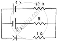
Find the current through the resistance R in figure if (a) R = 12Ω (b) R = 48Ω.

(Assume that the resistance of each diode is zero in forward bias and is infinity in reverse bias.)
When the base current in a transistor is changed from 30µA to 80µA, the collector current is changed from 1.0 mA to 3.5 mA. Find the current gain β.
A load resistor of 2kΩ is connected in the collector branch of an amplifier circuit using a transistor in common-emitter mode. The current gain β = 50. The input resistance of the transistor is 0.50 kΩ. If the input current is changed by 50µA. (a) by what amount does the output voltage change, (b) by what amount does the input voltage change and (c) what is the power gain?
An AC source is connected to a diode and a resistor in series. Is the current thorough the resistor AC or DC?
Choose the correct option.
Current through a reverse-biased p-n junction increases abruptly at:
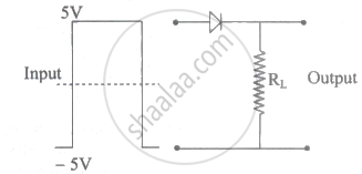
If in a p-n junction diode, a square input signal of 10 V is applied as shown Then the output signal across RL will be ______

