Topics
Rotational Dynamics
- Rotational Dynamics
- Circular Motion and Its Characteristics
- Applications of Uniform Circular Motion
- Vertical Circular Motion
- Moment of Inertia as an Analogous Quantity for Mass
- Radius of Gyration
- Theorems of Perpendicular and Parallel Axes
- Angular Momentum or Moment of Linear Momentum
- Expression for Torque in Terms of Moment of Inertia
- Conservation of Angular Momentum
- Rolling Motion
- Overview: Rotational Dynamics
Circular Motion
- Angular Displacement
- Angular Velocity
- Angular Acceleration
- Angular Velocity and Its Relation with Linear Velocity
- Uniform Circular Motion (UCM)
- Radial Acceleration
- Dynamics of Uniform Circular Motion - Centripetal Force
- Centrifugal Forces
- Banking of Roads
- Vertical Circular Motion Due to Earth’s Gravitation
- Equation for Velocity and Energy at Different Positions of Vertical Circular Motion
- Kinematical Equations for Circular Motion in Analogy with Linear Motion.
Gravitation
- Newton’s Law of Gravitation
- Periodic Time
- Kepler’s Laws
- Binding Energy and Escape Velocity of a Satellite
- Weightlessness
- Variation of ‘G’ Due to Lattitude and Motion
- Variation in the Acceleration>Variation in Gravity with Altitude
- Communication satellite and its uses
- Composition of Two S.H.M.’S Having Same Period and Along Same Line
Mechanical Properties of Fluids
- Fluid and Its Properties
- Thrust and Pressure
- Pressure of liquid
- Pressure Exerted by a Liquid Column
- Atmospheric Pressure
- Gauge Pressure and Absolute Pressure
- Hydrostatic Paradox
- Pascal’s Law
- Application of Pascal’s Law
- Measurement of Atmospheric Pressure
- Mercury Barometer (Simple Barometer)
- Open Tube Manometer
- Surface Tension
- Molecular Theory of Surface Tension
- Surface Tension and Surface Energy
- Angle of Contact
- Effect of Impurity and Temperature on Surface Tension
- Excess Pressure Across the Free Surface of a Liquid
- Explanation of Formation of Drops and Bubbles
- Capillarity and Capillary Action
- Fluids in Motion
- Critical Velocity and Reynolds Number
- Viscous Force or Viscosity
- Stokes’ Law
- Terminal Velocity
- Continuous and Discontinuous Functions
- Bernoulli's Equation
- Applications of Bernoulli’s Equation
- Overview: Mechanical Properties of Fluids
Angular Momentum
- Definition of M.I., K.E. of Rotating Body
- Rolling Motion
- Physical Significance of M.I (Moment of Inertia)
- Torque and Angular Momentum
- Theorems of Perpendicular and Parallel Axes
- M.I. of Some Regular Shaped Bodies About Specific Axes
Kinetic Theory of Gases and Radiation
- Gases and Its Characteristics
- Classification of Gases: Real Gases and Ideal Gases
- Mean Free Path
- Expression for Pressure Exerted by a Gas
- Root Mean Square (RMS) Speed
- Interpretation of Temperature in Kinetic Theory
- Law of Equipartition of Energy
- Specific Heat Capacity
- Absorption, Reflection, and Transmission of Heat Radiation
- Perfect Blackbody
- Emission of Heat Radiation
- Kirchhoff’s Law of Heat Radiation and Its Theoretical Proof
- Spectral Distribution of Blackbody Radiation
- Wien's Displacement Law
- Stefan-boltzmann Law of Radiation
- Overview: Kinetic Theory of Gases and Radiation
Thermodynamics
- Thermodynamics
- Thermal Equilibrium
- Measurement of Temperature
- Heat, Internal Energy and Work
- First Law of Thermodynamics
- Thermodynamic State Variables and Equation of State
- Thermodynamic Process
- Heat Engine
- Refrigerators and Heat Pumps
- Entropy and Second Law of Thermodynamics
- Carnot Cycle and Carnot Engine
- Overview: Thermodynamics
Oscillations
- Periodic and Oscillatory Motion
- Simple Harmonic Motion (S.H.M.)
- Differential Equation of Linear S.H.M.
- Projection of U.C.M.(Uniform Circular Motion) on Any Diameter
- Phase of K.E (Kinetic Energy)
- K.E.(Kinetic Energy) and P.E.(Potential Energy) in S.H.M.
- Composition of Two S.H.M.’S Having Same Period and Along Same Line
- Some Systems Executing Simple Harmonic Motion
Elasticity
- Eneral Explanation of Elastic Property
- Stress and Strain
- Hooke’s Law
- Elastic Energy
- Elastic Constants and Their Relation
- Determination of ‘Y’
- Behaviour of Metal Wire Under Increasing Load
- Application of Elastic Behaviour of Materials
Oscillations
- Oscillations
- Explanation of Periodic Motion
- Linear Simple Harmonic Motion (S.H.M.)
- Differential Equation of Linear S.H.M.
- Acceleration (a), Velocity (v) and Displacement (x) of S.H.M.
- Amplitude (A), Period (T) and Frequency (N) of S.H.M.
- Reference Circle Method
- Phase in S.H.M.
- Graphical Representation of S.H.M.
- Composition of Two S.H.M.’S Having Same Period and Along Same Line
- The Energy of a Particle Performing S.H.M.
- Simple Pendulum
- Angular S.H.M. and It's Differential Equation
- Damped Oscillations
- Free Oscillations, Forced Oscillations and Resonance Oscillations
- Periodic and Oscillatory Motion
- Overview: Oscillations
Surface Tension
- Molecular Theory of Surface Tension
- Surface Tension
- Capillarity and Capillary Action
- Effect of Impurity and Temperature on Surface Tension
Superposition of Waves
- Superposition of Waves
- Progressive Waves
- Reflection of Waves
- Stationary Waves
- Free and Forced Vibrations
- Harmonics and Overtones
- Sonometer
- Beats
- Characteristics of Sound
- Musical Instruments
- The Speed of a Travelling Wave
- Speed of Wave Motion
- Study of Vibrations of Air Columns
- Overview: Superposition of Waves
Wave Optics
- Introduction of Wave Optics
- Nature of Light
- Light as a Wave
- Huygens’ Theory
- Reflection of Light at a Plane Surface
- Refraction of Light at a Plane Boundary Between Two Media
- Polarization
- Interference
- Diffraction of Light
- Resolving Power
- Overview: Wave Optics
Wave Motion
- Wave Motion Introduction
- Simple Harmonic Progressive Waves,
- Reflection of Transverse and Longitudinal Waves
- Change of Phase
- Principle of Superposition of Waves
- Formation of Beats
- Beats
Electrostatics
- Concept of Electrostatics
- Application of Gauss' Law
- Electric Potential and Potential Difference
- Electric Potential Due to a Point Charge
- Equipotential Surfaces
- Electrical Energy of Two Point Charges and of a Dipole in an Electrostatic Field
- Free Charges and Bound Charges Inside a Conductor
- Combination of Capacitors
- Displacement Current
- Energy Stored in a Charged Capacitor
- Van De Graaff Generator
- Uniformly Charged Infinite Plane Sheet and Uniformly Charged Thin Spherical Shell (Field Inside and Outside)
- Overview: Electrostatics
Stationary Waves
- Study of Vibrations in a Finite Medium
- Formation of Stationary Waves on String
- Study of Vibrations of Air Columns
- Free and Forced Vibrations
- Forced Oscillations and Resonance
Current Electricity
- Current Electricity
- Kirchhoff’s Laws of Electrical Network
- Wheatstone Bridge
- Galvanometer
- Moving Coil Galvanometer
- Overview: Current Electricity
Kinetic Theory of Gases and Radiation
- Concept of an Ideal Gas
- Assumptions of Kinetic Theory of Gases
- Mean Free Path
- Derivation for Pressure of a Gas
- Degrees of Freedom
- Derivation of Boyle’s Law
- Thermal Equilibrium
- First Law of Thermodynamics
- Heat Engine
- Temperature and Heat
- Qualitative Ideas of Black Body Radiation
- Wien's Displacement Law
- Green House Effect
- Stefan's Law
- Maxwell Distribution
- Specific Heat Capacities - Gases
- Law of Equipartition of Energy
Wave Theory of Light
Magnetic Fields Due to Electric Current
- Magnetic Fields Due to Electric Current
- Magnetic force
- Cyclotron
- Helical Motion
- Magnetic Force on a Wire Carrying a Current
- Force on a Closed Circuit in a Magnetic Field
- Torque on a Current-Loop in a Uniform Magnetic Field
- Magnetic Dipole Moment
- Magnetic Potential Energy of a Dipole
- Biot-Savart Law
- Force of Attraction Between Two Long Parallel Wires
- Magnetic Field Produced by a Current in a Circular Arc of a Wire
- Applications of Biot-Savart's Law > Magnetic Field on the Axis of a Circular Current-Carrying Loop
- Magnetic Lines for a Current Loop
- Ampere's Law
- Applications of Ampere’s Circuital Law > Magnetic Field of a Toroidal Solenoid
- Overview: Magnetic Fields Due to Electric Current
Magnetic Materials
- Magnetic Materials
- Torque Acting on a Magnetic Dipole in a Uniform Magnetic Field
- Origin of Magnetism in Materials
- Magnetisation and Magnetic Intensity
- Magnetic Properties of Materials
- Classification of Magnetic Materials
- Hysteresis: Retentivity and Coercivity
- Permanent Magnet
- Magnetic Shielding
- Overview: Magnetic Materials
Interference and Diffraction
- Interference of Light
- Conditions for Producing Steady Interference Pattern
- Interference of Light Waves and Young’s Experiment
- Analytical Treatment of Interference Bands
- Measurement of Wavelength by Biprism Experiment
- Fraunhofer Diffraction Due to a Single Slit
- Rayleigh’s Criterion
- Resolving Power of a Microscope and Telescope
- Difference Between Interference and Diffraction
Electromagnetic Induction
- Electromagnetic Induction
- Faraday's Laws of Electromagnetic Induction
- Lenz's Law
- Flux of the Field
- Motional Electromotive Force (e.m.f.)
- Induced Emf in a Stationary Coil in a Changing Magnetic Field
- Generators
- Back Emf and Back Torque
- Induction and Energy Transfer
- Eddy Currents or Foucault Currents
- Self Inductance
- Energy Stored in a Magnetic Field
- Energy Density of a Magnetic Field
- Mutual Inductance
- Transformers
- Overview of Electromagnetic Induction
Electrostatics
- Mechanical Force on Unit Area of a Charged Conductor
- Energy Density of a Medium
- Concept of Condenser
- The Parallel Plate Capacitor
- Capacity of Parallel Plate Condenser
- Effect of Dielectric on Capacity
- Energy of Charged Condenser
- Condensers in Series and Parallel,
- Van-deGraaff Generator
Current Electricity
- Meter Bridge
AC Circuits
- AC Circuits
- Average and RMS Values
- Phasors
- Different Types of AC Circuits: AC Voltage Applied to a Resistor
- Different Types of AC Circuits: AC Voltage Applied to an Inductor
- Different Types of AC Circuits: AC Voltage Applied to a Capacitor
- Different Types of AC Circuits: AC Voltage Applied to a Series LCR Circuit
- Power in AC Circuit
- LC Oscillations
- Electric Resonance
- Sharpness of Resonance: Q Factor
- Choke Coil
- Overview: AC Circuits
Dual Nature of Radiation and Matter
- Dual Nature of Radiation and Matter
- The Photoelectric Effect
- Wave-particle Duality of Electromagnetic Radiation
- Photo Cell
- De Broglie Hypothesis
- Davisson and Germer Experiment
- Wave-particle Duality of Matter
- Overview: Dual Nature of Radiation and Matter
Magnetic Effects of Electric Current
Magnetism
Structure of Atoms and Nuclei
- Structure of the Atom and Nucleus
- Thomson’s Atomic Model
- Geiger-marsden Experiment
- Lord Rutherford’s Atomic model
- Atomic Spectra
- Bohr’s Atomic Model
- Atomic Nucleus
- Constituents of a Nucleus
- Isotopes
- Atomic and Nuclear Masses
- Size and Density of the Nucleus
- Mass Defect and Binding Energy
- Binding Energy Curve
- Forms of Energy > Nuclear Energy
- Nuclear Binding Energy
- Radioactive Decays
- Law of Radioactive Decay
- Overview: Structure of Atoms and Nuclei
Electromagnetic Inductions
- Electromagnetic Induction
- Self Inductance
- Mutual Inductance
- Transformers
- Need for Displacement Current
- Coil Rotating in Uniform Magnetic Induction
- A.C. Generator
- Reactance and Impedance
- LC Oscillations
- Inductance and Capacitance
- Resonant Circuits
- Power in AC Circuit
- Lenz’s Law and Conservation of Energy
Semiconductor Devices
- Basics of Semiconductor Devices
- p-n Junction Diode as a Rectifier
- Special Purpose Junction Diodes
- Bipolar Junction Transistor (BJT)
- Basics of Logic Gates
- Overview: Semiconductor Devices
Electrons and Photons
Atoms, Molecules and Nuclei
- Alpha-particle Scattering and Rutherford’s Nuclear Model of Atom
- Bohr’s Model for Hydrogen Atom
- Hydrogen Spectrum
- Atomic Masses and Composition of Nucleus
- Radioactivity
- Law of Radioactive Decay
- Atomic Mass, Mass - Energy Relation and Mass Defect
- Nuclear Binding Energy
- Nuclear Fusion – Energy Generation in Stars
- de-Broglie Relation
- Wave Nature of Matter
- Wavelength of an Electron
- Davisson and Germer Experiment
- Continuous and Characteristics X-rays
- Mass Defect and Binding Energy
Semiconductors
- Energy Bands in Solids
- Extrinsic Semiconductor
- Applications of n-type and p-type Semiconductors
- Special Purpose P-n Junction Diodes
- Semiconductor Diode
- Zener Diode as a Voltage Regulator
- I-V Characteristics of Led
- Transistor and Characteristics of a Transistor
- Transistor as an Amplifier (Ce-configuration)
- Transistor as a Switch
- Oscillators
- Digital Electronics and Logic Gates
Communication Systems
- Introduction
- Comparison between N-Type Semiconductor and P- Type Semiconductor
- Advantages
- Disadvantages
Semiconductor Devices
Semiconductors are tetravalent atoms called intrinsic semiconductors with conductivity between conductors and insulators. Adding impurities creates P-type and N-type semiconductors, a process called doping. Doped semiconductors are extrinsic. Current flows through both electrons and holes.
N type & P type Semiconductor Device
N-Type: These semiconductors are doped with pentavalent atoms, making electrons the majority charge carriers and holes the minority carriers. These donor atoms provide extra electrons. Common impurities used are antimony, arsenic, and phosphorus.
P-type: These semiconductors are doped with trivalent atoms, resulting in holes as the majority charge carriers and electrons as the minority carriers. These acceptor atoms create holes. Typical impurities include aluminium, boron, indium, and gallium.
PN Junction Diode & Barrier Potential
A semiconductor diode, like a valve diode, is formed by joining P-type and N-type semiconductors, creating a P-N junction. The P-type, with majority holes, acts as the anode, while the N-type, with majority electrons, acts as the cathode.
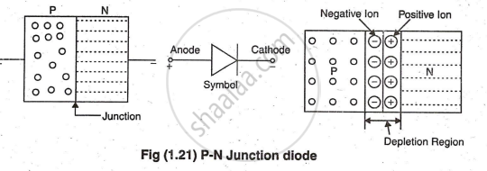
When a P-N junction forms, some electrons from the N-region cross over and fill holes in the P-region, creating positive ions in the N-region and negative ions in the P-region. This forms a depletion region with a barrier potential that opposes further electron and hole movement. The barrier potential is 0.7V for silicon diodes and 0.3V for germanium diodes.
Forward & Reverse Bias of PN Junction Diode
In forward bias, the P-N junction diode conducts with low resistance and almost acts like a closed switch. The negative terminal repels electrons in the N-region toward the junction, overcoming the potential barrier (0.7V for silicon, 0.3V for germanium). Electrons then move through the P-region and are collected by the positive terminal, while holes are attracted to the negative terminal, facilitating current flow.
This is another way of connecting diode, P- region (anode) to negative terminal and N-region (cathode) to positive terminal of the battery, and then it is called as 'reverse bias'. In this condition the width of potential barrier increases and restricts the flow of majority carriers. A very small amount of current flows due to minority carriers and is called leakage current.
The above explanation concludes that current flow through diode is possible only in one direction, in forward bias and not in reverse bias.
Half Wave Rectifier & It’s Working (Applications of diode)
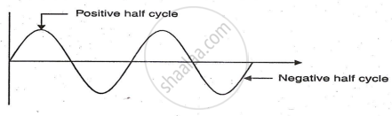
AC Voltage consists of two half cycles, as shown in Fig . The upper half cycle is known as the positive half cycle, and the lower cycle is known as the negative half cycle.
A half-wave rectifier is a simple and low-cost rectifier circuit. It is used where high-quality DC is not required, for example, to operate a nightlight or radio circuit.
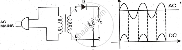
Working:
i) Refer to the circuit diagram and waveforms. In the first half cycle of AC voltage, when terminal A of the transformer is positive relative to terminal B (fig. 1.27a), the diode becomes forward-biased and acts as a closed switch. Current flows from terminal A through RL to terminal B, producing an output voltage across RL like the positive half cycle of the AC input
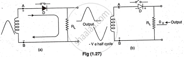
ii) In the negative half cycle, terminal B is positive relative to terminal A (fig. 1.27b). The diode becomes reverse biased, acting as an open switch, and blocking current flow.
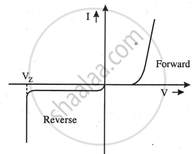
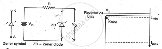
Zener Diode (Types of diodes)
A Zener diode provides stable voltage in reverse bias and is available in voltages from 2 to 200V. In reverse bias, as voltage increases, the current remains minimal until reaching the breakdown voltage (Vz). At this point, current increases sharply, but the voltage across the diode stays constant, even with further voltage increases, ensuring stable voltage regulation. Zener diodes are used in DC power supplies as a voltage regulator or in special circuits to stabilize the voltage.
Light Emitting Diode (LED) & Photo Diode
LEDs, made from Gallium, Arsenic, and Phosphorus, emit light in forward bias instead of heat like normal diodes. Recombination of holes and electrons at the P-N junction produces light. LEDs come in red, green, and yellow. LEDs are used in 7-segment displays, watches, calculators, digital meters, and power supply indicators. A series resistor is needed to limit current and prevent damage.
Photo diode conducts when light is incident on it. Photodiodes, made with cadmium selenide (CdSe), cadmium sulphide (CdS), germanium, and silicon, operate in reverse bias. They generate electron-hole pairs and current when exposed to light, with current depending on light intensity. It is used in computer punch card; light detectors, sound reproduction of film projector and light operated switches.
