Advertisements
Advertisements
प्रश्न
The current−voltage characteristic of an ideal p-n junction diode is given by \[i = i_0 ( e^{eV/KT} - 1)\] where, the drift current i0 equals 10 µA. Take the temperature T to be 300 K. (a) Find the voltage V0 for which \[e^{eV/kT} = 100 .\]One can neglect the term 1 for voltages greater than this value. (b) Find an expression for the dynamic resistance of the diode as a function of V for V > V0. (c) Find the voltage for which the dynamic resistance is 0.2 Ω.
(Use Planck constant h = 4.14 × 10⁻¹⁵ eV-s, Boltzmann constant k = 8·62 × 10-5 eV/K.)
उत्तर
(a) The current‒voltage relationship of a diode is given by
\[i = i_0 ( e^{eV/kT - 1} )\]
For a large value of voltage, 1 can be neglected.
\[i \approx i_0 e^{eV/kT}\]
Again, we need to find the voltage at which
\[e^{eV/kT} = 100\]
\[\Rightarrow \frac{eV}{kT} = \text{ln }100\]
\[ \Rightarrow V = \frac{\text{ ln }100 \times \text{ kT }}{e}\]
\[ \Rightarrow V = \frac{2 . 303 \times \log 100 \times 8 . 62 \times {10}^{- 5} \times 300}{e}\]
\[ \Rightarrow V=0.12\] V
(b) Given:-
\[i = i_0 ( e^{eV/kT - 1} ) ...........(1)\]
We know that the dynamic resistance of a diode is the rate of change of voltage w.r.t. current.
i.e.
\[R = \frac{d V}{\text{d i}}\]
As the exponential factor dominates the factor of 1, we can neglect this factor.
Now, on differentiating eq. (1) w.r.t. V, we get
\[\frac{\text{di}}{\text{dV}} = i_0 \frac{e}{kT} e^{eV/kT} \]
\[ \Rightarrow \frac{1}{R} = \frac{e i_0}{kT} e^{eV/kT} \]
\[ \Rightarrow R = \frac{kT}{e i_0} e^{- eV/kT} ............(2)\]
(c) Given:-
R = 2 Ω
On substituting this value in eq. (2), we get
\[2 = \frac{8 . 62 \times {10}^{- 5} \times 300}{e \times 10 \times {10}^{- 6}} e^{- eV/8 . 62 \times {10}^{- 5} \times 300} \]
\[ \Rightarrow V = 0 . 25 \] V
APPEARS IN
संबंधित प्रश्न
In an unbiased p-n junction, holes diffuse from the p-region to n-region because ______.
In a p-n junction diode, the current I can be expressed as
I = `"I"_0 exp ("eV"/(2"k"_"BT") - 1)`
where I0 is called the reverse saturation current, V is the voltage across the diode and is positive for forward bias and negative for reverse bias, and I is the current through the diode, kBis the Boltzmann constant (8.6×10⁻⁵ eV/K) and T is the absolute temperature. If for a given diode I0 = 5 × 10⁻¹² A and T = 300 K, then
(a) What will be the forward current at a forward voltage of 0.6 V?
(b) What will be the increase in the current if the voltage across the diode is increased to 0.7 V?
(c) What is the dynamic resistance?
(d) What will be the current if reverse bias voltage changes from 1 V to 2 V?
Write the two processes that take place in the formation of a p-n junction.
A zener diode is fabricated by heavily doping both p- and n- sides of the junction. Explain, why?
Explain briefly with the help of necessary diagrams, the reverse biasing of a p-n junction diode. Also draw characteristic curves.
A student wants to use two p-n junction diodes to convert alternating current into direct current. Draw the labelled circuit diagram she would use and explain how it works.
Draw a circuit diagram to study the input and output characteristics of an n-p-n transistor in its common emitter configuration. Draw the typical input and output characteristics.
When a p-type impurity is doped in a semiconductor, a large number of holes are created, This does not make the semiconductor charged. But when holes diffuse from the p-side to the n-side in a p-n junction, the n-side gets positively charged. Explain.
The diffusion current in a p-n junction is
A hole diffuses from the p-side to the n-side in a p-n junction. This means that
In a p-n junction with open ends,
(a) there is no systematic motion of charge carries
(b) holes and conduction electrons systematically go from the p-side to n-side and from the n-side to p-side respectively
(c) there is no net charge transfer between the two sides
(d) there is a constant electric field near the junction.
In a p.n junction, the depletion region is 400 nm wide and an electric field of 5 × 10⁵ V m−1 exists in it. (a) Find the height of the potential barrier. (b) What should be the minimum kinetic energy of a conduction electron which can diffuse from the n-side to the p-side?
The drift current in a p-n junction is 20.0 µA. Estimate the number of electrons crossing a cross section per second in the depletion region.
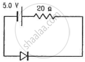
Calculate the current through the circuit and the potential difference across the diode shown in figure. The drift current for the diode is 20 µA.

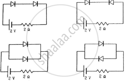
Find the currents through the resistance in the circuits shown in figure.

(Assume that the resistance of each diode is zero in forward bias and is infinity in reverse bias.)
An AC source is connected to a diode and a resistor in series. Is the current thorough the resistor AC or DC?
In a semiconductor diode, the barrier potential offers opposition to only ______.
p-n junction diode is formed
