Advertisements
Advertisements
प्रश्न
What happens when a forward bias is applied to a p-n junction?
उत्तर
In forward biasing, the applied voltage mostly drops across the depletion region, and the voltage drop across the p-side and n-side of the junction is negligible. The direction of the applied voltage (V) is opposite to the built-in potential Vo. As a result, the depletion layer width decreases and the barrier height is reduced. The effective barrier height under forward bias is (Vo − V).
APPEARS IN
संबंधित प्रश्न
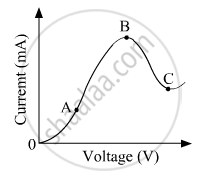
The graph shown in the figure represents a plot of current versus voltage for a given semiconductor. Identify the region, if any, over which the semiconductor has a negative resistance.

Show on a graph, the variation of resistivity with temperature for a typical semiconductor.
Basic materials used in the present solid state electronic devices like diode, transistor, ICs, etc are ______.
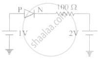
The current through an ideal PN-junction shown in the following circuit diagram will be:

Use a transistor as an amplition
Can the potential barrier across a p-n junction be measured by simply connecting a voltmeter across the junction?
Draw V-I characteristics of a p-n Junction diode.
Differentiate between the threshold voltage and the breakdown voltage for a diode.
With reference to a semiconductor diode, define the depletion region.
What is meant by forward biasing of a semiconductor diode?
