Advertisements
Online Mock Tests
Chapters
2: Current Electricity
3: Magnetism and magnetic effects of electric current
4: Electromagnetic Induction And Alternating Current
5: Electromagnetic waves
6: Ray Optics
7: Wave Optics
8: Dual Nature of Radiation and Matter
9: Atomic and Nuclear physics
▶ 10: Electronics and Communication
11: Recent Developments in Physics
![Samacheer Kalvi solutions for Physics - Volume 1 and 2 [English] Class 12 TN Board chapter 10 - Electronics and Communication - Shaalaa.com](/images/physics-volume-1-and-2-english-class-12-tn-board_6:5f2b1b2038084cf381bfa42c826a928c.jpg "Samacheer Kalvi solutions for Physics - Volume 1 and 2 [English] Class 12 TN Board chapter 10 - Electronics and Communication")
Advertisements
Solutions for Chapter 10: Electronics and Communication
Below listed, you can find solutions for Chapter 10 of Tamil Nadu Board of Secondary Education Samacheer Kalvi for Physics - Volume 1 and 2 [English] Class 12 TN Board.
Samacheer Kalvi solutions for Physics - Volume 1 and 2 [English] Class 12 TN Board 10 Electronics and Communication Evaluation [Pages 246 - 250]
Multiple choice questions
The barrier potential of a silicon diode is approximately, ____________.
0.7 V
0.3 V
2.0 V
2.2 V
Doping a semiconductor result in
The decrease in mobile charge carriers
The change in chemical properties
The change in the crystal structure
The breaking of the covalent bond
In an unbiased p-n junction, the majority of charge carriers (that is, holes) in the p-region diffuse into the n-region because of
the potential difference across the p-n junction
the higher hole concentration in p-region than that in n-region
the attraction of free electrons of n-region
the higher concentration of electrons in the n-region than that in the p-region
If a positive half-wave rectified voltage is fed to a load resistor, for which part of a cycle there will be current flow through the load?
0° – 90°
90° – 180°
0° – 180°
0° – 360°
The zener diode is primarily used as ____________.
Rectifier
Amplifier
Oscillator
Voltage regulator
The principle based on which a solar cell operates is ____________.
Diffusion
Recombination
Photovoltaic action
Carrier flow
The light emitted in an LED is due to
Recombination of charge carriers
Reflection of light due to lens action
Amplification of light falling at the junction
Large current capacity
The barrier potential of a p-n junction depends on
(i) type of semiconductor material
(ii) amount of doping
(iii) temperature
Which one of the following is correct?
(i) and (ii) only
(ii) only
(ii) and (iii) only
(i), (ii) and (iii)
To obtain sustained oscillation in an oscillator,
Feedback should be positive
Feedback factor must be unity
Phase shift must be 0 or 2π
All the above
If the input to the NOT gate is A = 1011, its output is ____________.
0100
1000
1100
0011
Which one of the following represents forward bias diode?
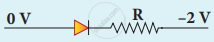
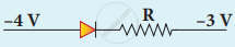
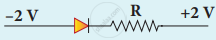
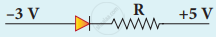
The given electrical network is equivalent to
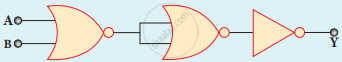
AND gate
OR gate
NOR gate
NOT gate
The output of the following circuit is 1 when the input ABC is
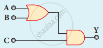
101
100
110
010
The variation of frequency of carrier wave with respect to the amplitude of the modulating signal is called ____________.
Amplitude modulation
Frequency modulation
Phase modulation
Pulse width modulation
The frequency range of 3 MHz to 30 MHz is used for ____________.
Ground wave propagation
Space wave propagation
Sky wave propagation
Satellite communication
Short Answer Questions
Define forbidden energy gap.
Why is temperature co-efficient of resistance negative for semiconductor?
What do you mean by doping?
Distinguish between intrinsic and extrinsic semiconductors.
A diode is called a unidirectional device. Explain.
What do you mean by leakage current in a diode?
Draw the input and output waveforms of a full wave rectifier.
Distinguish between avalanche breakdown and Zener breakdown.
Give the Barkhausen conditions for sustained oscillations.
Explain the current flow in an NPN transistor.
What are logic gates?
Explain the need for a feedback circuit in a transistor oscillator.
Write a short note on diffusion current across the p-n junction.
What is meant by biasing?
Mention the types of biasing.
Why can’t we interchange the emitter and collector even though they are made up of the same type of semiconductor material?
Why are NOR and NAND gates called universal gates?
Define barrier potential.
What is rectification?
List the applications of light emitting diode.
Give the principle of solar cells.
What is an integrated circuit?
What is modulation?
Define bandwidth of transmission system.
What do you mean by skip distance?
Give applications of RADAR.
What is mobile communication?
Explain centre frequency or resting frequency in frequency modulation.
What does RADAR stand for?
Long Answer Questions
Elucidate the formation of n-type extrinsic semiconductors.
Explain the formation of depletion region and barrier potential in PN junction diode.
Draw the circuit diagram of a half wave rectifier and explain its working.
Explain the construction and working of a full-wave rectifier.
What is an LED? Give the principle of its operation with a diagram.
Write notes on the photodiode.
Explain the working principle of a solar cell. Mention its applications.
Sketch the static characteristics of a common emitter transistor and bring out the essential features of input and output characteristics.
Transistor functions as a switch. Explain.
Describe the function of a transistor as an amplifier with the neat circuit diagram. Sketch the input and output wave forms.
Give circuit symbol, logical operation, truth table, and Boolean expression of AND gate.
Give circuit symbol, logical operation, truth table, and Boolean expression of OR gate.
Give circuit symbol, logical operation, truth table, and Boolean expression of NOT gate.
Give circuit symbol, logical operation, truth table, and Boolean expression of NAND gate.
Give circuit symbol, logical operation, truth table, and Boolean expression of NOR gate.
Give circuit symbol, logical operation, truth table, and Boolean expression of EX-OR gate.
State and prove De Morgan’s first and second theorem.
Explain the amplitude modulation with necessary diagrams.
Explain the basic elements of the communication system with the necessary block diagram.
Explain the ground wave propagation and space wave propagation of electromagnetic waves through space.
Fiber optic communication is gaining popularity among the various transmission media. - justify
List out the advantages and limitations of frequency modulation.
What is meant by satellite communication?
Give the applications of satellite communication.
Numerical Problems
The given circuit has two ideal diodes connected as shown in the figure below. Calculate the current flowing through the resistance R1.
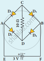
Four silicon diodes and a 10 Ω resistor are connected as shown in the figure below. Each diode has a resistance of 1 Ω. Find the current flows through the 10 Ω resistor.
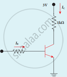
Assuming VCEsat = 0.2 V and β = 50, find the minimum base current (IB) required to drive the transistor given in the figure to saturation.
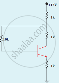
A transistor of α = 0.99 and VBE = 0.7 V is connected in the common-emitter configuration as shown in the figure. If the transistor is in the saturation region, find the value of collector current.
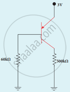
In the circuit shown in the figure, the BJT has a current gain (β) of 50. For an emitter-base voltage VEB = 600 mV, calculate the emitter-collector voltage VEC (in volts).
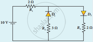
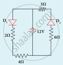
Determine the current flowing through 3 Ω and 4 Ω resistors of the circuit given below. Assume that diodes D1 and D2 are ideal diodes.
Prove the following Boolean expression using the laws and theorems of Boolean algebra.
`("A" + "B") ("A" + overline"B")` = A
Prove the following Boolean expression using the laws and theorems of Boolean algebra.
`"A" (overline"A" + "B")` = AB
Prove the following Boolean expression using the laws and theorems of Boolean algebra.
(A + B) (A + C) = A + BC
Verify the given Boolean equation A + `overline"A""B"` = A + B using truth table.
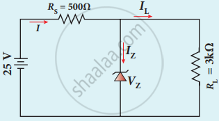
In the given figure of a voltage regulator, a Zener diode of breakdown voltage 10 V is employed. Determine the current through the load resistance, the total current and the current through the diode. Use diode approximation.
Write down the Boolean equation for the output Y of the given circuit and give its truth table.

Solutions for 10: Electronics and Communication
Samacheer Kalvi solutions for Physics - Volume 1 and 2 [English] Class 12 TN Board chapter 10 - Electronics and Communication
Shaalaa.com has the Tamil Nadu Board of Secondary Education Mathematics Physics - Volume 1 and 2 [English] Class 12 TN Board Tamil Nadu Board of Secondary Education solutions in a manner that help students grasp basic concepts better and faster. The detailed, step-by-step solutions will help you understand the concepts better and clarify any confusion. Samacheer Kalvi solutions for Mathematics Physics - Volume 1 and 2 [English] Class 12 TN Board Tamil Nadu Board of Secondary Education 10 (Electronics and Communication) include all questions with answers and detailed explanations. This will clear students' doubts about questions and improve their application skills while preparing for board exams.
Further, we at Shaalaa.com provide such solutions so students can prepare for written exams. Samacheer Kalvi textbook solutions can be a core help for self-study and provide excellent self-help guidance for students.
Concepts covered in Physics - Volume 1 and 2 [English] Class 12 TN Board chapter 10 Electronics and Communication are Introduction to Electronics, Types of Semiconductors, Diodes, Bipolar Junction Transistor (BJT), Digital Electronics, Boolean Algebra, De Morgan’s Theorem, Introduction to Communication System, Modulation, The Elements of an Electronic Communication System, Antenna Size, Propagation of Electromagnetic Waves, Satellite Communication, Fibre Optic Communication, Radar and Applications, Mobile Communication, Internet, Global Positioning System, Application of Information and Communication Technology (ICT).
Using Samacheer Kalvi Physics - Volume 1 and 2 [English] Class 12 TN Board solutions Electronics and Communication exercise by students is an easy way to prepare for the exams, as they involve solutions arranged chapter-wise and also page-wise. The questions involved in Samacheer Kalvi Solutions are essential questions that can be asked in the final exam. Maximum Tamil Nadu Board of Secondary Education Physics - Volume 1 and 2 [English] Class 12 TN Board students prefer Samacheer Kalvi Textbook Solutions to score more in exams.
Get the free view of Chapter 10, Electronics and Communication Physics - Volume 1 and 2 [English] Class 12 TN Board additional questions for Mathematics Physics - Volume 1 and 2 [English] Class 12 TN Board Tamil Nadu Board of Secondary Education, and you can use Shaalaa.com to keep it handy for your exam preparation.
