Advertisements
Advertisements
Question
The drift current in a p-n junction is
Options
from the n-side to the p-side
from the p-side to the n-side
from the p-side to the side if the junction is forward-biased and the opposite direction if it is reverse-biased
from the p-side to the n-side if the junction is forward-baised and in the opposite direction if it is reverse-biased.
Solution
from the n-side to the p-side
After the diffusion of majority charge carriers across a p‒n junction, an electric field is set up because of the accumulation of immobile ions at the junction. These further oppose the motion of majority charge carriers across the junction. As a result, electrons from the p region start moving to the n region and holes from the n region start moving to the p region. This constitutes the drift current. As the direction of the current is opposite to the direction of the motion of the electrons, the direction of the drift current is from the n side to the p side.
In forward biasing, there is no movement of electrons from the p region to the n region and of holes from the n region to the p region. Hence, there is not drift current.
APPEARS IN
RELATED QUESTIONS
In an unbiased p-n junction, holes diffuse from the p-region to n-region because ______.
In a p-n junction diode, the current I can be expressed as
I = `"I"_0 exp ("eV"/(2"k"_"BT") - 1)`
where I0 is called the reverse saturation current, V is the voltage across the diode and is positive for forward bias and negative for reverse bias, and I is the current through the diode, kBis the Boltzmann constant (8.6×10⁻⁵ eV/K) and T is the absolute temperature. If for a given diode I0 = 5 × 10⁻¹² A and T = 300 K, then
(a) What will be the forward current at a forward voltage of 0.6 V?
(b) What will be the increase in the current if the voltage across the diode is increased to 0.7 V?
(c) What is the dynamic resistance?
(d) What will be the current if reverse bias voltage changes from 1 V to 2 V?
Write the two processes that take place in the formation of a p-n junction.
A zener diode is fabricated by heavily doping both p- and n- sides of the junction. Explain, why?
Mention the important considerations required while fabricating a p-n junction diode to be used as a Light Emitting Diode (LED). What should be the order of band gap of an LED if it is required to emit light in the visible range?
The drift current in a reverse-biased p-n junction is increased in magnitude if the temperature of the junction is increased. Explain this on the basis of creation of hole-electron pairs.
If the two ends of a p-n junction are joined by a wire,
In a p-n junction,
(a) new holes and conduction electrons are produced continuously throughout the material
(b) new holes and conduction electrons are produced continuously throughout the material except in the depletion region
(c) holes and conduction electrons recombine continuously throughout the material
(d) holes and conduction electrons recombine continuously throughout the material except in the depletion region.
A semiconducting device is connected in a series circuit with a battery and a resistance. A current is found to pass through the circuit. If the polarity of the battery is reversed, the current drops to almost zero. the device may be
(a) an intrinsic semiconductor
(b) a p-type semiconductor
(c) an n-type semiconductor
(d) a p-n junction
The potential barrier existing across an unbiased p-n junction is 0.2 volt. What minimum kinetic energy a hole should have to diffuse from the p-side to the n-side if (a) the junction is unbiased, (b) the junction is forward-biased at 0.1 volt and (c) the junction is reverse-biased at 0.1 volt?
When a p-n junction is reverse-biased, the current becomes almost constant at 25 µA. When it is forward-biased at 200 mV, a current of 75 µA is obtained. Find the magnitude of diffusion current when the diode is
(a) unbiased,
(b) reverse-biased at 200 mV and
(c) forward-biased at 200 mV.
The drift current in a p-n junction is 20.0 µA. Estimate the number of electrons crossing a cross section per second in the depletion region.
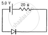
Calculate the current through the circuit and the potential difference across the diode shown in figure. The drift current for the diode is 20 µA.

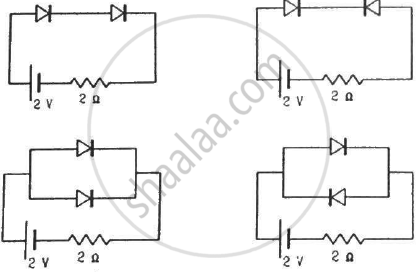
Find the currents through the resistance in the circuits shown in figure.

(Assume that the resistance of each diode is zero in forward bias and is infinity in reverse bias.)
Choose the correct option.
Current through a reverse-biased p-n junction increases abruptly at:
Answer in detail.
Discuss the effect of external voltage on the width of depletion region of a p-n junction.
The depletion layer in the p-n junction diode is caused by ______.
p-n junction diode is formed
The formation of the depletion region in a p-n junction diode is due to ______.
