Advertisements
Advertisements
Question
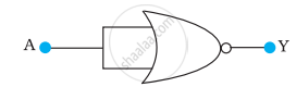
Draw the schematic symbols for AND, OR, NOT and NAND gate
Solution

APPEARS IN
RELATED QUESTIONS
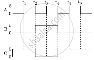
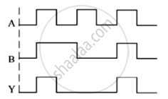
The following figure shows the input waveforms (A, B) and the output waveform (Y) of a gate. Identify the gate, write its truth table and draw its logic symbol.
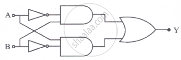
You are given the two circuits as shown in following figure. Show that circuit
- acts as OR gate while the circuit
- acts as AND gate.
(a)
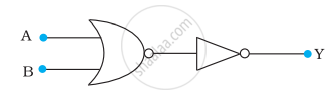
(b)
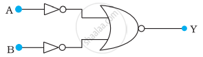
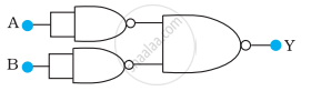
You are given two circuits as shown in following figure, which consist of NAND gates. Identify the logic operation carried out by the two circuits.
(a)
(b)
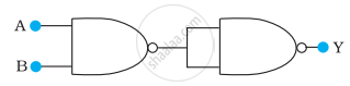
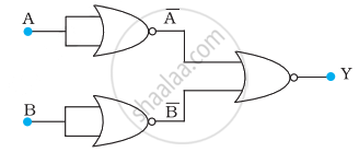
Write the truth table for circuit given in figure below consisting of NOR gates and identify the logic operation (OR, AND, NOT) which this circuit is performing.
(Hint: A = 0, B = 1 then A and B inputs of second NOR gate will be 0 and hence Y=1. Similarly work out the values of Y for other combinations of A and B. Compare with the truth table of OR, AND, NOT gates and find the correct one.)
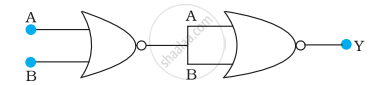
Write the truth table for the circuits given in following figure consisting of NOR gates only. Identify the logic operations (OR, AND, NOT) performed by the two circuits.
(a)
(b)
Answer the following question :
Distinguish between digital and analogue signals.
The output of an OR gate is connected to both the inputs of a NAND gate Draw the logic circuit of this combinaion of getes and write its truth table.
Let \[X = A \overline{ BC} + B\overline{ CA} + C\overline{AB } .\] Evaluate X for A = 1, B = 0, C = 1.
Let \[X = A \overline{ BC} + B\overline{ CA} + C\overline{AB } .\] Evaluate X for A = B = C = 0.
The amplification factor of a triode operating in the linear region depends strongly on ____________ .
Why are NOR gates considered as universal gates?
Draw the truth table of a NOR gate.
Draw a diagram to show how NAND gates can be combined to obtain an OR gate. (Truth table is not, required)
Useful Constants and Relations:
| 1. | Charge of a proton | (e) | =1.6 × 10⁻¹⁹C |
| 2. | Planck's constant | (h) | = 6·6 × 10-34 Js |
| 3. | Mass of an electron | (m) | = 9·1× 10-31 kg |
| 4. | Permittivity of vacuum | (∈0) | =8 · 85 × 10-12 Fm-1 |
| 5. | `(1/(4pi∈_0))` | =9 ×10⁹ mF-1 | |
| 6. | Permeability of vacuum | (μ0) | = 4π × 10-7 Hm-1 |
| 7. | `((mu_0)/(4pi))` | =1 × 10⁻⁷ Hm-1 | |
| 8. | Speed of light in vacuum | (c) | = 3× 10⁸ ms-1 |
| 9. | Unified atomic mass unit | (u) |
= 931 MeV |
| 10. | Electron volt | (leV) | = 1.6 × 10⁻¹⁹ J |
With the help of a diagram, show how you can use several NAND gates to obtain an OR gate.
Useful Constants and Relations :
| 1. Speed of Light in Vacuum | (c) = 3.00 x 10⁸ m/s |
| 2. Charge of a proton | (e) = 1.60 x 10⁻¹⁹C |
| 3. Planck's Constant | (h) = 6.6 x 10⁻³⁴ Js |
| 4. Permeability of vacuum | (μ0) = 4π x 10-7 Hm-1 |
| 5. Electron Volt | (1eV ) = 1.6 x 10 |
| 6. Unified Atomic Mass Unit | (1u) = 931 MeV |
| (π) = 3.14 | |
| ( ln 2 ) = 0.693 |
The output of 2-input or gate is zero only when its
An oscillator is nothing but an amplifier with
Which logic gate is similar to a function of two series switches?
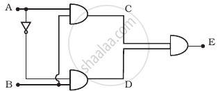
The truth table for the following logic circuit is:
For the given circuit, the input digital signals are applied at terminals A, B, and C. What would be the output at terminal y?
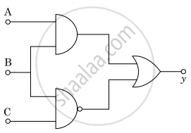
For the given circuit, the input digital signals are applied at the terminals A, B and C. What would be the output at the terminal y?
Truth table for the given circuit (Figure) is ______.
How would you set up a circuit to obtain NOT gate using a transistor?
An X-OR gate has following truth table:
| A | B | Y |
| 0 | 0 | 0 |
| 0 | 1 | 1 |
| 1 | 0 | 1 |
| 1 | 1 | 0 |
It is represented by following logic relation `Y = barA.B + A.barB`. Build this gate using AND, OR and NOT gates.
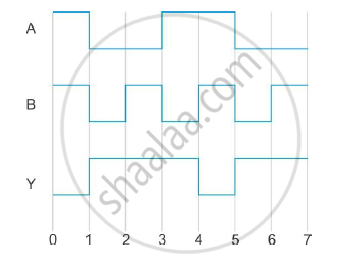
A logic gate circuit has two inputs A and B and output Y. The voltage waveforms of A, B and Y are shown below.
The logic gate circuit is ______.
