Advertisements
Advertisements
प्रश्न
With reference to semiconductor devices, define a p-type semiconductor and a Zener diode.
उत्तर
When a trivalent impurity like aluminium, indium, boron, gallium, etc., is doped with pure germanium
(or silicon) , then the conductivity of the crystal increases due to its deficiency of electrons i.e., holes and such a crystal is said to be p-type semiconductor while the impurity atoms are called acceptors.
A Zener diode is a reverse biased heavily doped p - n junction diode, which is operated in the breakdown region, where the current is limited by both external resistance and power dissipation of the diode.
APPEARS IN
संबंधित प्रश्न
With the help of neat labelled circuit diagram explain the working of half wave rectifier using semiconductor diode. Draw the input and output waveforms.
Draw its I – V characteristics of photodiode
The dynamic plate resistance of a triode value is 10 kΩ. Find the change in the plate current if the plate voltage is changed from 200 V to 220 V.
Diffusion in a p-n junction is due to ______.
The nature of binding for a crystal with alternate and evenly spaced positive and negatively ions is
In the circuit shown in figure, if the diode forward voltage drop is 0.3 V, the voltage difference between A and B is ______.

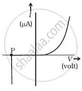
 (a) |
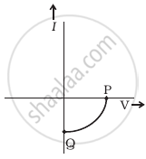
 (b) |
- Name the type of a diode whose characteristics are shown in figure (A) and figure (B).
- What does the point P in figure (A) represent?
- What does the points P and Q in figure (B) represent?
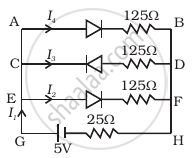
If each diode in figure has a forward bias resistance of 25 Ω and infinite resistance in reverse bias, what will be the values of the current I1, I2, I3 and I4?

Write the property of a junction diode which makes it suitable for rectification of ac voltages.
With reference to a semiconductor diode, define the depletion region.
