Advertisements
Advertisements
प्रश्न
Explain the working of P-N junction diode in forward and reverse biased mode.
उत्तर
If a germanium crystal or silicon crystal is doped during manufacture in such a way that half of it is p-type and other half is n-type, we get p-n junction.

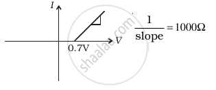
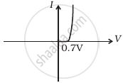
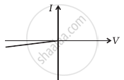
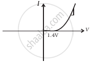
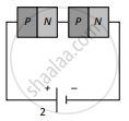
(a) Forward biased: A battery is connected across p-n junction diode such that, p-type is connected to positive terminal and n-type is connected to negative terminal, then it is called forward biased. The potential difference applied should be more than 0.3 V for germanium and more than 0.7 V for silicon. Then holes from p-type region and electrons from n-type region moves towards barrier and it decreases width and height of
barrier. Hence an electric current flows through circuit. When applied potential is zero, then current also equal to zero. When P.D. Increases the current is also increases but very slowly. When applied P.D. is more than potential barrier, current in creases rapidly. This voltage is called knee voltage. The forward biased voltage at which the current through diode increases rapidly is called knee voltage
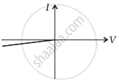
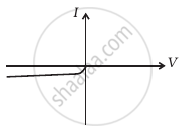
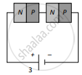
b) Reversed biased : A battery is connected across p-n junction diode such that, p-type is connected to negative terminal and n-type is connected to positive terminal, then it is called reversed biased. The holes from p type region and electrons from n-type region moves away from junction and it increases width and height of barrier. Hence there is no flow of an electric current in ideal case. In actual case current is very small (inμA) . The width of potential barrier increases and diode offer very high resistance. The very small current flows through circuit is called as reverse current. If reversed bias voltage increased then the kinetic energy of electrons increases. At certain reversed bias voltage the K.E. of electrons increases enough and they knock out the electrons from semiconductor atoms\ Therefore current suddenly increase. That certain reversed bias voltage is called as breakdown voltage. At breakdown voltage the current increases suddenly and destroy the junction permanently. The reversed bas voltage at which P-N junction breaks and current suddenly increases is called as breakdown voltage.
APPEARS IN
संबंधित प्रश्न
When a forward bias is applied to a p-n junction, it ______.
Draw its I – V characteristics of photodiode
With reference to semiconductor devices, define a p-type semiconductor and a Zener diode.
What is the use of Zener diode?
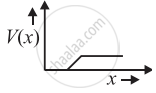
Plot a graph showing variation of current versus voltage for the material GaAs ?
With reference to semi-conductors answer the following :
(i) What is the change in the resistance of the semi-conductor with increase in temperature ?
(ii) Name the majority charge carriers in n-type semi-conductor.
(iii) What is meant by doping ?
A triode value operates at Vp = 225 V and Vg = −0.5 V.
The plate current remains unchanged if the plate voltage is increased to 250 V and the grid voltage is decreased to −2.5 V. Calculate the amplification factor.
With reference to a semiconductor diode, what is meant by:
(i) Forward bias
(ii) Reverse bias
(iii) Depletion region
Answer the following question.
Why photodiodes are required to operate in reverse bias? Explain.
Basic materials used in the present solid state electronic devices like diode, transistor, ICs, etc are ______.
We use alloys for making standard resistors because they have ____________.
What are the applications of p - n Junction diode?
The current through an ideal PN-junction shown in the following circuit diagram will be:
In a semiconductor diode, the barrier potential offers opposition to only
Avalanche breakdown is due to ______.
In the circuit shown in figure, if the diode forward voltage drop is 0.3 V, the voltage difference between A and B is ______.

A Zener of power rating 1 W is to be used as a voltage regulator. If zener has a breakdown of 5 V and it has to regulate voltage which fluctuated between 3 V and 7 V, what should be the value of Rs for safe operation (Figure)?

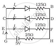
If each diode in figure has a forward bias resistance of 25 Ω and infinite resistance in reverse bias, what will be the values of the current I1, I2, I3 and I4?
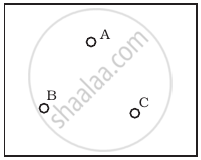
Consider a box with three terminals on top of it as shown in figure (a):
 (a) |
Three components namely, two germanium diodes and one resistor are connected across these three terminals in some arrangement. A student performs an experiment in which any two of these three terminals are connected in the circuit shown in figure (b).
 (b) |
The student obtains graphs of current-voltage characteristics for unknown combination of components between the two terminals connected in the circuit. The graphs are
(i) when A is positive and B is negative
 (c) |
(ii) when A is negative and B is positive
 (d) |
(iii) When B is negative and C is positive
|
(e) |
(iv) When B is positive and C is negative
 (f) |
(v) When A is positive and C is negative
 (g) |
(vi) When A is negative and C is positive
 (h) |
From these graphs of current-voltage characteristics shown in figure (c) to (h), determine the arrangement of components between A, B and C.
The graph of potential barrier versus width of depletion region for an unbiased diode is shown in graph A. In comparison to A, graphs B and C are obtained after biasing the diode in different ways. Identify the type of biasing in B and C and justify your answer
| ‘A’ | ‘B’ | ‘C’ |
 |
 |
 |
Write the property of a junction diode which makes it suitable for rectification of ac voltages.
Explain the formation of the barrier potential in a p-n junction.
Answer the following giving reasons:
A p-n junction diode is damaged by a strong current.
Describe briefly the following term:
minority carrier injection in forward biasing.
Read the following paragraph and answer the questions that follow.
| A semiconductor diode is basically a pn junction with metallic contacts provided at the ends for the application of an external voltage. It is a two-terminal device. When an external voltage is applied across a semiconductor diode such that the p-side is connected to the positive terminal of the battery and the n-side to the negative terminal, it is said to be forward-biased. When an external voltage is applied across the diode such that the n-side is positive and the p-side is negative, it is said to be reverse-biased. An ideal diode is one whose resistance in forward biasing is zero and the resistance is infinite in reverse biasing. When the diode is forward biased, it is found that beyond forward voltage called knee voltage, the conductivity is very high. When the biasing voltage is more than the knee voltage the potential barrier is overcome and the current increases rapidly with an increase in forward voltage. When the diode is reverse biased, the reverse bias voltage produces a very small current of about a few microamperes which almost remains constant with bias. This small current is a reverse saturation current. |
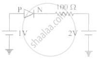
- In the given figure, a diode D is connected to an external resistance R = 100 Ω and an emf of 3.5 V. If the barrier potential developed across the diode is 0.5 V, the current in the circuit will be:

(a) 40 mA
(b) 20 mA
(c) 35 mA
(d) 30 mA - In which of the following figures, the pn diode is reverse biased?
(a)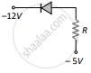
(b)
(c)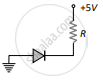
(d)
- Based on the V-I characteristics of the diode, we can classify the diode as:
(a) bilateral device
(b) ohmic device
(c) non-ohmic device
(d) passive element
OR
Two identical PN junctions can be connected in series by three different methods as shown in the figure. If the potential difference in the junctions is the same, then the correct connections will be:
(a) in the circuits (1) and (2)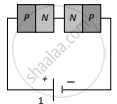
(b) in the circuits (2) and (3)
(c) in the circuits (1) and (3)
(d) only in the circuit (1) 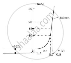
The V-I characteristic of a diode is shown in the figure. The ratio of the resistance of the diode at I = 15 mA to the resistance at V = -10 V is
(a) 100
(b) 106
(c) 10
(d) 10-6
With reference to a semiconductor diode, define the depletion region.
With reference to a semiconductor diode, define the potential barrier.
What is meant by forward biasing of a semiconductor diode?
