Advertisements
Advertisements
प्रश्न
A plate current of 10 mA is obtained when 60 volts are applied across a diode tube. Assuming the Langmuir-Child relation \[i_p \infty V_p^{3/2}\] to hold, find the dynamic resistance rp in this operating condition.
उत्तर
According to Lamgmuir-Child Law,
the relation between plate current (ip) and the plate voltage (Vp) is given by
\[i_p = C {V_p}^{3/2} ............(1)\]
Differentiating equation (1) with respect Vp, we get:-
\[\frac{d i_p}{d V_p} = \frac{3}{2}C {V_p}^{1/2} ............(2)\]
Dividing (2) and (1), we get:-
\[\frac{1}{i_p}\frac{d i_p}{d v_p} = \frac{3/2C {V_p}^{1/2}}{C {V_p}^{3/2}}\]
\[ \Rightarrow \frac{1}{i_p} . \frac{d i_p}{d v_p} = \frac{3}{2 V_p}\]
The dynamic resistance is given by:-
\[\frac{d v_p}{d i_p} = \frac{2 V_p}{3 i_p}\]
\[ r_p = \frac{2 V_p}{3 i_p}\]
\[ r_p = \frac{2 \times 60}{3 \times 10 \times {10}^{- 3}}\]
\[ r_p = 4 \times {10}^3 = 4 k\Omega\]
APPEARS IN
संबंधित प्रश्न
(i) Explain with the help of a diagram the formation of depletion region and barrier potential in a pn junction.
With the help of neat labelled circuit diagram explain the working of half wave rectifier using semiconductor diode. Draw the input and output waveforms.
What causes the setting up of high electric field even for small reverse bias voltage across the diode?
Why is a zener diode considered as a special purpose semiconductor diode?
The gain factor of an amplifier in increased from 10 to 12 as the load resistance is changed from 4 kΩ to 8 kΩ. Calculate (a) the amplification factor and (b) the plate resistance.
With reference to a semiconductor diode, what is meant by:
(i) Forward bias
(ii) Reverse bias
(iii) Depletion region
What are the applications of p - n Junction diode?
The drift current in a p-n junction is from the ______.
Use a transistor as an amplition
The expected energy of the electron at absolute zero is called:-
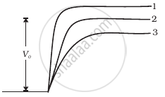
In Figure, Vo is the potential barrier across a p-n junction, when no battery is connected across the junction ______.
In the circuit shown in figure, if the diode forward voltage drop is 0.3 V, the voltage difference between A and B is ______.

In the depletion region of a diode ______.
- there are no mobile charges.
- equal number of holes and electrons exist, making the region neutral.
- recombination of holes and electrons has taken place.
- immobile charged ions exist.
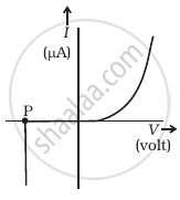 (a) |
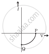 (b) |
- Name the type of a diode whose characteristics are shown in figure (A) and figure (B).
- What does the point P in figure (A) represent?
- What does the points P and Q in figure (B) represent?
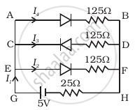
If each diode in figure has a forward bias resistance of 25 Ω and infinite resistance in reverse bias, what will be the values of the current I1, I2, I3 and I4?
Consider a box with three terminals on top of it as shown in figure (a):
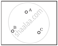 (a) |
Three components namely, two germanium diodes and one resistor are connected across these three terminals in some arrangement. A student performs an experiment in which any two of these three terminals are connected in the circuit shown in figure (b).
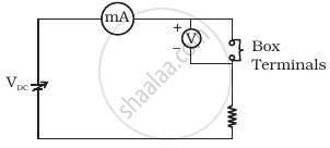 (b) |
The student obtains graphs of current-voltage characteristics for unknown combination of components between the two terminals connected in the circuit. The graphs are
(i) when A is positive and B is negative
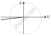 (c) |
(ii) when A is negative and B is positive
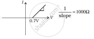 (d) |
(iii) When B is negative and C is positive
|
(e) |
(iv) When B is positive and C is negative
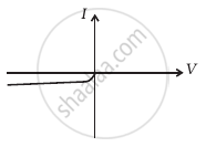 (f) |
(v) When A is positive and C is negative
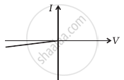 (g) |
(vi) When A is negative and C is positive
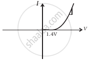 (h) |
From these graphs of current-voltage characteristics shown in figure (c) to (h), determine the arrangement of components between A, B and C.
Draw V-I characteristics of a p-n Junction diode.
Write the property of a junction diode which makes it suitable for rectification of ac voltages.
Draw the circuit arrangement for studying V-I characteristics of a p-n junction diode in (i) forward biasing and (ii) reverse biasing. Draw the typical V-I characteristics of a silicon diode.
