Topics
Electronic Components/ Study of Components and Circuits
- Introduction to Electronic Components
- Classification Of Components
- Resistors
- Types of Resistors
- Capacitors
- Types of Capacitors
- Inductors
- Basics of Transformers
- Basics of Semiconductor Devices
- PN Junction Diode
- Half Wave Rectifier
- Types of diodes
- Transistors
- Transistor Amplifier
- Basic of Transistor as a Switch
- Switch Mode power Supply (SMPS)
- Classification of IC’S
Logic Gates and Sequential Circuit
- Introduction of Logic gates and sequential circuits
- Basics of Logic Gates
- Types of gates
- Odd/Even Parity
- DE-MORGAN'S Theorem
- NAND Gate is an Universal Building Block
- HALF ADDER AND FULL ADDER
- Multiplexers
- Demultiplexer
- Encoder
- Decoder
- FLIP-FLOPS
- Counters
- Shift Registers
Functional Hardware of Pc
Peripheral Devices
- Introduction to flip-flop
- R-S Flip-flop
- D-Flip flop
- J-K Flip-flop
- T Flip-flop
FLIP-FLOPS
A flip-flop, or bistable multivibrator, is essential in digital circuits like registers, counters, and memory. Constructed using gates, it serves as a memory element with two states: "set" (1) or "reset" (0).
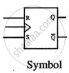
R-S Flip-Flop
It is the basic circuit, which requires for constructing the other flip-flop circuits. It has two inputs 'S' and 'R' and two outputs denoted by 'Q' and `bar Q` where Q is called normal output and `bar Q` is called as complementary output.
Truth Table & Symbol: 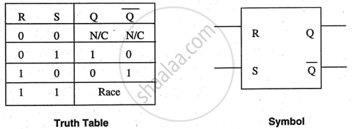
R-S Flip Flop using Gates
Due to integrated circuit technology, the flip-flop can be fabricated in the form of gates. Since NOR and NAND are building blocks, the working of a gate circuit can be explained with their 'disable' and 'enable' state.
Disable State: If one NOR gate input is 1(high), the output is 0, regardless of the other input. This is the Disable state of NOR gate.
Enable State: If one NAND gate input is 0(low), the output is 1, regardless of the other input. This is the Enable state of NAND gate.
Working of NOR Flip-Flop:
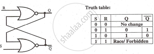
Case 1: When S = 0 and R = 0, the flip-flop remains in its last state ("No Change").
Case 2: When S = 0 and R = 1, the upper NOR gate is disabled, producing Q = 0. The lower NOR gate then produces Q = 1 ("Reset").
Case 3: When S = 1 and R = 0, the lower NOR gate is disabled, producing Q = 0. The upper NOR gate then produces Q = 1 ("Set").
Case 4: When S = 1 and R = 1, both NOR gates are disabled, leading to an unpredictable state ("Race" or forbidden state).
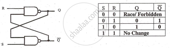
The NAND S flip-flop works similarly, considering the "Enable" state. When S = 1 and R = 1, there is no change (N/C). When S = 0 and R = 0, both NAND gates try to enable, causing a "Race" condition. This is the main difference
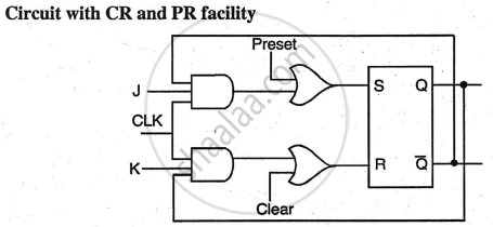
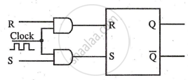
Clocked R-S Flip-Flop
Theoretical circuits transmit inputs to outputs without control. Practically, a control input is added to R and S inputs for synchronization with the main circuit, using a common "CLOCK" signal. Fig. (2.23) shows a clocked R-S flip-flop and its truth table.
Circuit
Truth Table
|
CLK |
R |
S |
Q | `bar Q` |
|
0 |
X |
X |
N/C |
N/C |
|
1 |
0 |
0 |
N/C |
N/C |
|
1 |
0 |
1 |
1 |
0 |
|
1 |
1 |
0 |
0 |
1 |
|
1 |
1 |
1 |
Race |
Race |
The flip-flop is enabled only when the clock is high; if the clock is low (0), the flip-flop remains in its last state (N/C). When the clock is absent or low, both AND gates are disabled, resulting in no input to the internal R-S flip-flop, thus no change in output. This state is indicated as "X," meaning "don't care."
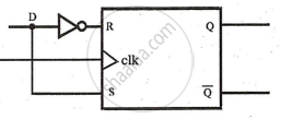
Clocked D Flip-Flop (Delay Flip-Flop)
The D flip-flop can be derived from R-S flip-flop. The R-S flip-flop has two drawbacks:
- It requires two separate inputs 'S' and 'R'
- The possibility of forbidden or race condition.
These drawbacks are eliminated in D flip-flop; this flip-flop needs a single data input 'D'
Circuit
Truth Table
|
CLK |
D |
Q |
`bar Q`
|
|
0 |
X |
N/C |
N/C |
|
1 |
0 |
0 |
1 |
|
1 |
1 |
1 |
0 |
When CLK = 1, D = 1 sets the flip-flop (Q=1, Q=0); D = 0 resets it. D flip-flops are used in registers and ring counters.
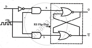
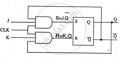
J-K Flip Flop (JUMP and KEY Flip-Flop)
The J-K flip-flop, built from an R-S flip-flop, toggles when J = 1 and K = 1, changing to the opposite state with each clock pulse.
Circuit
Truth Table
|
CLK |
J |
K |
Q |
`bar Q`
|
|
0 |
X |
X |
N/C |
N/C |
|
1 |
0 |
0 |
N/C |
N/C |
|
1 |
1 |
0 |
1 |
0 |
|
1 |
0 |
1 |
0 |
1 |
|
1 |
1 |
1 |
Toggle |
Toggle |
In counter circuits, J-K flip-flops use edge-triggered clocks, either positive or negative edge. Fig (2.27) shows the J-K flip-flop symbol with terminals. Edge triggering, preferred to avoid false triggers, is achieved with an R-C differentiator circuit.
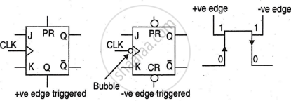
In a positive edge-triggered flip-flop, the output changes at the rising clock edge (0 to 1). In a negative edge-triggered flip-flop, it changes at the falling edge (1 to 0). The J-K flip-flop has PR (PRESET) to set the output and CR (CLEAR) to reset the output independently of J, K, and the clock.