Topics
Introduction to Microprocessors and Organization of 8085
Instruction Set and Programming of 8085
Introdcution to Inted X-86 Family
Introduction to Microcontroller
Networking Technology
- Introduction to Networking
- Types of Networks
- Multiplexing
- Study of Transmission media
- Coaxial cable (Cable Media)
- Twisted pair cable
- Fiber Optic Cable
- Unbounded (Wireless) Media
- Access Methods
- Network Topologies
- Ethernet (Network Architectures)
- Token-Ring (Network Architectures)
- Internet protocols
- Introduction to connectivity devices
- Address & Data Bus
- Data Address & Instruction Register
- Instruction Decoder
- Arithmetic and Logic unit(ALU) & Accumulator
- Program Counter & Stack Pointer
- Timing and control unit
- Control Inputs and Outputs
- Bus Buffers and Latches
- Status Register
Block Diagram of Generic Microprocessor
Before going for the study of 8085, let's first understand the detailed block diagram of generic microprocessor i.e. a general microprocessor. The block diagram is shown in figure below.
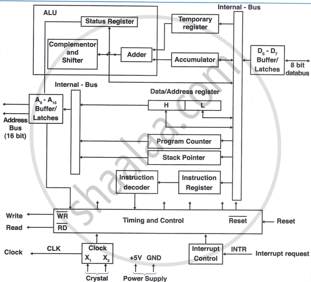
Address & Data Bus
The address bus consists of 16 lines labeled A0 to A15 and is unidirectional, meaning data flows only from the microprocessing unit (MPU) to peripheral devices. The MPU uses this bus to specify memory or device locations. Each location in a computer system has a unique address. The 16-bit address bus can handle 65,536 (or 64K) distinct addresses.
The data bus consists of 8 lines that allow data to flow both ways between the MPU and memory or peripheral devices. The MPU uses the data bus to transfer data. These lines can carry 8-bit data, ranging from 00 to FF, which equals 256 possible values. Microprocessors with an 8-bit data bus are known as 8-bit microprocessors.
Data Address & Instruction Register
The data address register consists of two 8-bit registers, labeled H (high order byte) and L (low order byte). These registers can be used independently or together as a pair. They are general-purpose registers capable of storing data. When used together, they can store a 16-bit address.
Instruction Register is an 8 bit register. The first byte (i.e. 8 bits) of an instruction is stored in this register
Instruction Decoder
This unit interprets the contents of the instruction register. It determines the exact steps to be followed in executing the entire instruction and directs the control section accordingly.
Arithmetic and Logic unit(ALU) & Accumulator
ALU performs arithmetic and logic operations. This unit also performs rotate operation. The operations in this unit affect the status register. The results from ALU are placed in accumulator.
Accumulator is 8 bit register. Many times, it is treated as a part of ALU. This register is used to store 8 - bit data and in arithmetic and logic operations, the result is stored in accumulator.
Program Counter & Stack Pointer
Program counter is a 16 bit register. It contains the address from where the next instruction is to be executed. It can be incremented or reset by the control section. Transfer instructions can modify contents of Program Counter
The stack pointer is a 16-bit register that holds the address of a memory location called the stack. The stack is a series of memory locations in read/write memory specified by the programmer and used for temporary storage.
Timing and control unit
This section gets signals from the instruction decoder to identify the type of instruction to execute. It also uses information from the status register for conditional branching. Timing and control signals are sent throughout the microprocessor to manage instruction execution, and external control signals are generated as well.
Control Inputs and Outputs
Reset and interrupt request (INTR) are control inputs for general microprocessors. Activating reset stops all internal operations and clears the program counter, allowing program execution to start from address 0000H. Activating INTR interrupts normal instruction execution to run a different set of instructions, called a service routine, after which the microprocessor resumes its previous operations.
Control outputs include write, read, and clock lines. An external crystal connected between X1 and X2 generates the clock signal for internal use and synchronization of the entire system. The read (RD) signal enables the input buffer, allowing data on the data lines to be written to memory or I/O locations. Both RD and WR are active-low control signals.
Bus Buffers and Latches
A latch is a type of flip-flop used to store one bit of information. To prevent accidental input changes and control output availability, tri-state buffers can be used with latches. Writing to the latch is done by enabling the buffer.
Status Register
The status register, also known as the flag register, contains flip-flops that are set or reset based on the data in the accumulator. A typical microprocessor has two flags: Zero and Carry. If an arithmetic operation, like addition, results in a sum larger than 8 bits, the Carry flag is set to one. If the operation results in zero, the Zero flag is set.
